TA8423F 查看數據表(PDF) - Toshiba
零件编号
产品描述 (功能)
生产厂家
TA8423F Datasheet PDF : 13 Pages
| |||
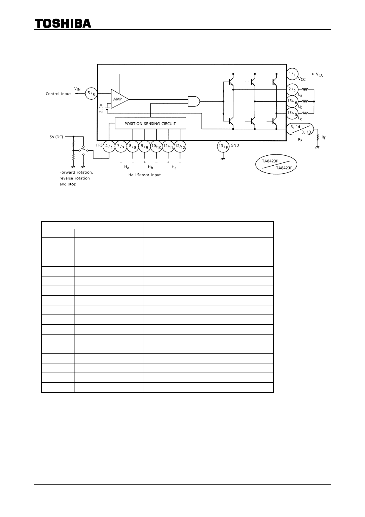
BLOCK DIAGRAM
TA8423P/F
PIN FUNCTION
PIN No.
P
F
1
1
2
2
3
3
4
4
5
5
6
6
7
7
8
8
9
9
10
10
11
11
12
12
13
FIN
14
13
15
15
16
16
SYMBOL
VCC
La
RF
FRS
VIN
N.C
Ha+
Ha−
Hb+
Hb−
Hc+
Hc−
GND
RF
Lc
Lb
FUNCTION DESCRIPTION
Power supply input terminal.
a−phase drive output terminal.
Output current detection terminal.
Forward / Reverse control terminal.
Control Amp. positive input terminal.
Non Connection.
a−phase Hall Amp. positive input terminal.
a−phase Hall Amp. negative input terminal.
b−phase Hall Amp. positive input terminal.
b−phase Hall Amp. negative input terminal.
c−phase Hall Amp. positive input terminal.
c−phase Hall Amp. negative input terminal.
GND terminal.
Output current detection terminal.
c−phase drive output terminal.
b−phase drive output terminal.
2
2001-06-13
Share Link: 