TSM221(1997) 查看數據表(PDF) - STMicroelectronics
零件编号
产品描述 (功能)
生产厂家
TSM221
(Rev.:1997)
(Rev.:1997)
STMicroelectronics
TSM221 Datasheet PDF : 11 Pages
| |||
TSM221
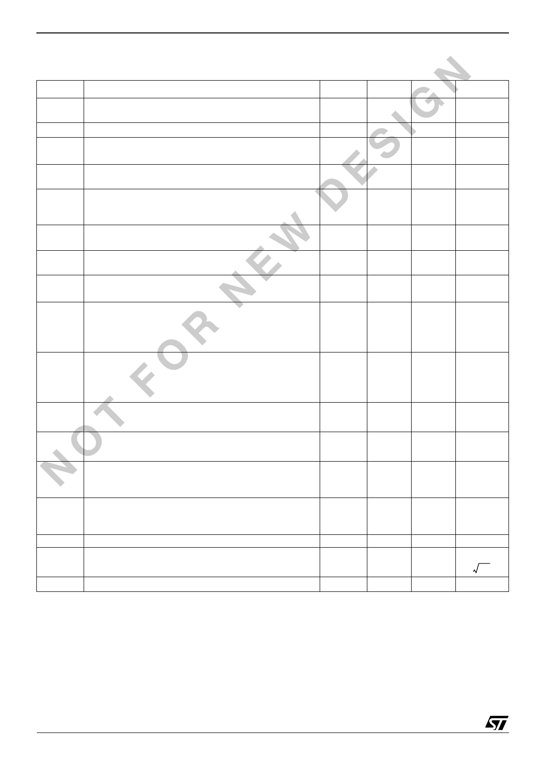
OPERATIONAL AMPLIFIERS
ELECTRICAL CHARACTERISTICS
VCC+
=
3V,
VC
-
C
=
0V,
RL,CL
connected
to
VCC/2,
Tamb
=
25oC
(unless
otherwise
specified)
Symbol
Parameter
Vio Input Offset Voltage
DVio
Iio
Input Offset Voltage Drift
Input Offset Current - (note 1)
Iib Input Bias Current - (note 1)
Avd Large Signal Voltage Gain
ICC
CMR
SVR
VOH
Total Supply Current- (note 2)
Common Mode Rejection Ratio
Supply Voltage Rejection Ratio
High Level Output Voltage
R1 connected to VCC/2
VOL Low Level Output Voltage
R1 connected to VCC/2
Io
Isink
GBP
Output Short Circuit Current
Output Sink Current
Gain Bandwidth Product
SR Slew Rate
∅m Phase Margin
en Equivalent Input Noise Voltage
Test Condition
Tmin. ≤ Tamb ≤ Tmax.
Tmin. ≤ Tamb ≤ Tmax.
Tmin. ≤ Tamb ≤ Tmax.
RL = 10kΩ, VO = 1.5V to 3.5V
Tmin. ≤ Tamb ≤ Tmax.
No load
Vic = 0 to 3V, Vo = 1.5V
VCC+ = 2.7V to 3.3V, VO = VCC /2
RL = 10k
RL = 600Ω
RL = 100Ω
RL = 10k
RL = 600Ω
RL = 100Ω
Vo = VCC-
Vo = VCC+
AVCL = 100, RL = 10k,
CL = 100pF, f = 100kHz
AVCL = 1, RL = 10k,
CL = 100pF, Vi = 1.3V to 1.7V
Rs = 100Ω, f = 1kHz
Min.
3
2
50
2.90
2.30
20
20
Typ.
5
1
1
10
415
70
80
2.96
2.60
2
30
300
900
40
40
0.8
0.3
30
30
Max.
10
12
100
200
150
300
600
70
400
Cs Channel Separation
f = 1kHz
120
Note 1 : Maximum values including unavoidable inaccuracies of the industrial test.
Note 2 : Op-amps and comparators
Unit
mV
µV/oC
pA
pA
V/mV
µA
dB
dB
V
mV
mA
mA
MHz
V/µs
Degrees
nV
√Hz
dB
4/11
Share Link: 