MC100EL31D 查看數據表(PDF) - ON Semiconductor
零件编号
产品描述 (功能)
生产厂家
MC100EL31D Datasheet PDF : 9 Pages
| |||
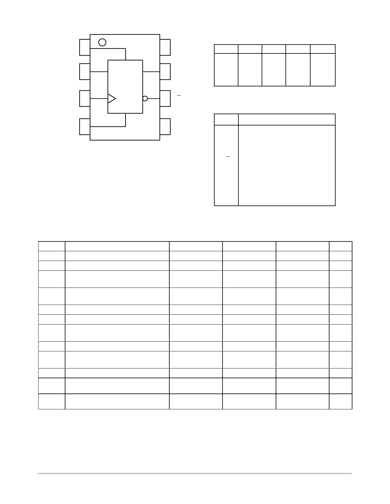
MC10EL31, MC100EL31
S1
D2
S
D
8 VCC
7Q
CLK 3
R4
6Q
R
5 VEE
Figure 1. Logic Diagram and Pinout Assignment
Table 1. TRUTH TABLE
D
S*
R*
CLK
L
L
L
Z
H
L
L
Z
X
H
L
X
X
L
H
X
X
H
H
X
Z = LOW to HIGH Transition
* Pins will default low when left open.
Table 2. PIN DESCRIPTION
PIN
FUNCTION
Q
L
H
H
L
Undef
S
D
R
CLK
Q, Q
VCC
VEE
EP
ECL Set Input
ECL Data Input
ECL Reset Input
ECL Clock Input
ECL Data Outputs
Positive Supply
Negative Supply
Exposed pad must be connected to a
sufficient thermal conduit. Electrically
connect to the most negative supply
or leave floating open.
Table 3. MAXIMUM RATINGS
Symbol
Parameter
Condition 1
Condition 2
Rating
Unit
VCC
PECL Mode Power Supply
VEE
NECL Mode Power Supply
VI
PECL Mode Input Voltage
NECL Mode Input Voltage
Iout
Output Current
VEE = 0 V
VCC = 0 V
VEE = 0 V
VCC = 0 V
Continuous
Surge
VI VCC
VI VEE
8
V
−8
V
6
V
−6
V
50
mA
100
mA
TA
Operating Temperature Range
Tstg
Storage Temperature Range
qJA
Thermal Resistance (Junction−to−Ambient) 0 lfpm
500 lfpm
SOIC−8
SOIC−8
−40 to +85
−65 to +150
190
130
°C
°C
°C/W
°C/W
qJC
Thermal Resistance (Junction−to−Case) Standard Board
SOIC−8
qJA
Thermal Resistance (Junction−to−Ambient) 0 lfpm
500 lfpm
TSSOP−8
TSSOP−8
41 to 44
185
140
°C/W
°C/W
°C/W
qJC
Thermal Resistance (Junction−to−Case) Standard Board
TSSOP−8
qJA
Thermal Resistance (Junction−to−Ambient) 0 lfpm
500 lfpm
DFN8
DFN8
41 to 44 ± 5%
129
84
°C/W
°C/W
°C/W
Tsol
Wave Solder
Pb <2 to 3 sec @ 248°C
Pb−Free <2 to 3 sec @ 260°C
265
°C
265
Stresses exceeding Maximum Ratings may damage the device. Maximum Ratings are stress ratings only. Functional operation above the
Recommended Operating Conditions is not implied. Extended exposure to stresses above the Recommended Operating Conditions may affect
device reliability.
http://onsemi.com
2
Share Link: 