UPD75P3036GK 查看數據表(PDF) - NEC => Renesas Technology
零件编号
产品描述 (功能)
生产厂家
UPD75P3036GK Datasheet PDF : 64 Pages
| |||
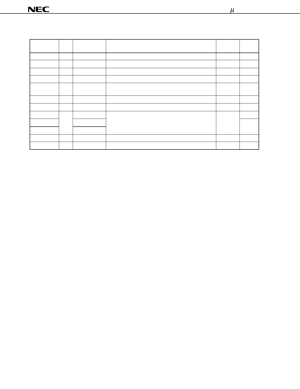
µPD75P3036
3.2 Non-port Pins (2/2)
Pin name
I/O
Alternate
function
Function
Status I/O circuit
after reset type
S12 to S23 Output
—
S24 to S31 Output BP0 to BP7
COM0 to COM3 Output
—
VLC0 to VLC2
—
—
BIAS
Output
—
LCDCLNote 2
SYNCNote 2
Output P30/MD0
Output P31/MD1
Segment signal output
Note 1
G-A
Segment signal output
Note 1
H-A
Common signal output
Note 1
G-B
Power source for LCD driver
—
—
Output for external split resistor cut
High
—
impedance
Clock output for driving external expansion driver
Input
E-B
Clock output for synchronization of external expansion driver Input
E-B
AN0 to AN5
AN6
AN7
Input
—
P82
P83
Analog signal input for A/D converter
Input
Y
Y-B
AVREF
AVSS
—
—
A/D converter reference voltage
—
—
A/D converter reference GND potential
—
Z-N
—
Z-N
Notes 1. The VLCX (X = 0, 1, 2) shown below are selected as the input source for the display outputs.
S12 to S31: VLC1, COM0 to COM2: VLC2, COM3: VLC0
2. These pins are provided for future system expansion. Currently, only P30 and P31 are used.
10
Share Link: 