UPD77115GK-9EU 查看數據表(PDF) - NEC => Renesas Technology
零件编号
产品描述 (功能)
生产厂家
UPD77115GK-9EU Datasheet PDF : 56 Pages
| |||
µPD77115, 77115A
1. PIN FUNCTION
Because the pin numbers differ depending on the package, refer to the diagram of the package to be used.
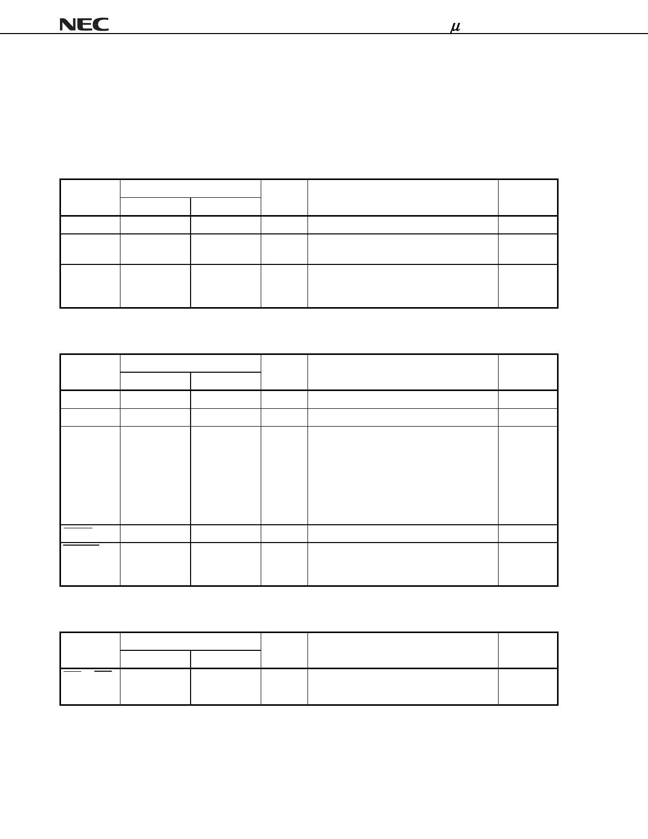
1.1 Pin Function Description
• Power supply
Pin Name
IVDD
EVDD
GND
Pin No.
80-pin FBGA 80-pin TQFP
A4,D7,H7
37,53,72
A1,A3,E8,F1,
G9,H2,H4
12,21,30,43,51,
75,80
B4,C4,D9,E3,
E6,H1,H5,H9,
J2,J8
8,18,22,31,
38,42,52,54,
73,76
I/O
Function
−
Power to DSP core (+2.5 V)
−
Power to I/O pins (+3 V)
−
Ground
Shared by:
−
−
−
• System control
Pin Name
Pin No.
80-pin FBGA 80-pin TQFP
CLKIN
F8
50
CLKOUT
E9
49
PLL0 to PLL3 E2,D2,E1,D4 11,10,9,7
RESET
A6
66
WAKEUP
B5
71
I/O
Function
Shared by:
Input
Output
Input
Input
Input
System clock input
Internal system clock output
PLL multiple rate setting pin
PLL3 to PLL0:
0000 : x16, 0001 : x1, 0010 : x2, 0011 : x3,
0100 : x4, 0101 : x5, 0110 : x6, 0111 : x7,
1000 : x8, 1001 : x9, 1010 : x10, 1011 : x11,
1100 : x12, 1101 : x13, 1110 : x14,
1111 : x15
Internal system reset signal input
Stop mode release signal input.
• When this pin is asserted active, the stop
mode is released.
−
−
P4 to P7
−
−
• Interrupt
Pin Name
Pin No.
80-pin FBGA 80-pin TQFP
INT1 to INT4 B6,A5,C5,D6 70,69,68,67
I/O
Function
Input
External maskable interrupt input.
• Detected at the falling edge.
Shared by:
−
10
Data Sheet U14867EJ5V0DS
Share Link: 