FX019DW 查看數據表(PDF) - CML Microsystems Plc
零件编号
产品描述 (功能)
生产厂家
FX019DW Datasheet PDF : 7 Pages
| |||
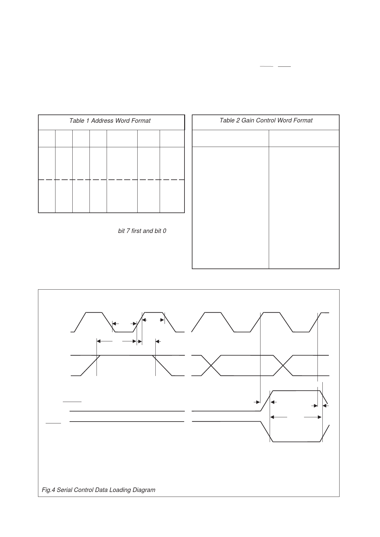
Control Data and Timing
The gain of each amplifier block (Channel 1 to
Channel 4) in the FX019 is set by a separate 8-bit
data word ( bit 7 to bit 0 ). This 8-bit word, consisting
of 4 Address bits (bit 7 to bit 4) and 4 Gain Control
bits (bit 3 to bit 0), is loaded to the Control Data Input
in serial format using the external data clock.
Data is loaded to the FX019 on the rising edge of the
Serial Clock. Loaded data is executed on the falling
(rising) edge of the Load/Latch (Load/Latch) pulse.
Table 1 shows the format of each 4-bit Address word,
Table 2 shows the format of each Gain Control word
with Figure 4 describing the data loading operation and
timing.
Table 1 Address Word Format
Bit 7 Bit 6 Bit 5 Bit 4 Channel
MSB
LSB Selected
1
0
0
0
1
1
0
0
1
2
1
0
1
0
3
1
0
1
1
4
Chip Chip
Select Number
0
0
Chip
0
1
0
1
1
0
0
1
1
1
0
1
2
1
1
1
0
3
1
1
1
1
4
1
1
Chip
1
2
1
Data Loading
The 8-bit data word is loaded bit 7 first and bit 0 last.
Bit 7 must be a logic “1” to address the chip.
If bit 7 in the word is a logic “0” that 8-bit word will not be
executed. The Chip Select input permits the use of two
devices in a system; To facilitate this, Bit 6 can be either
a logic “0” or “1.” Figure 4 (below) shows the timing
information required to load and operate this device.
Table 2 Gain Control Word Format
Bit 3 Bit2 Bit 1 Bit 0 Stage 1, 2, 3 Stage 4
MSB
LSB
(0.43dB) (2.0dB)
0
0
0
0
0
0
0
1
0
0
1
0
0
0
1
1
0
1
0
0
0
1
0
1
0
1
1
0
0
1
1
1
1
0
0
0
1
0
0
1
1
0
1
0
1
0
1
1
1
1
0
0
1
1
0
1
1
1
1
0
1
1
1
1
OFF
-3.0
-2.571
-2.143
-1.714
-1.286
-0.857
-0.428
0
0.428
0.857
1.286
1.714
2.143
2.571
3.0
OFF
-14.0dB
-12.0
-10.0
-8.0
-6.0
-4.0
-2.0
0
2.0
4.0
6.0
8.0
10.0
12.0
14.0
SERIAL DATA CLOCK
SERIAL DATA IN
(ONE 8-BIT WORD)
t PWL
t DS
t PWH
tDH
Logic ’1’
Loaded
First
BIT 7
BIT 6 BIT 1
8th
Clock
Pulse
Loaded Last
BIT 0
LOAD/LATCH
LOAD/LATCH
Timing
tPWH
Serial Clock "High" Pulse Width
tPWL
Serial Clock "Low" Pulse Width
Fig.4 Serial Control Data Loading Diagram
tDS
Data Set-up Time
tDH
Data Hold Time
tLLD
Load/Latch Delay
4
t LLD
t LLW
tLLW
Load/Latch Pulse Width
tLLO
Load/Latch Over Time
Next
Clock
Pulse
t LLO
Share Link: 