STL24N60M2 查看數據表(PDF) - STMicroelectronics
零件编号
产品描述 (功能)
生产厂家
STL24N60M2
STMicroelectronics
STL24N60M2 Datasheet PDF : 15 Pages
| |||
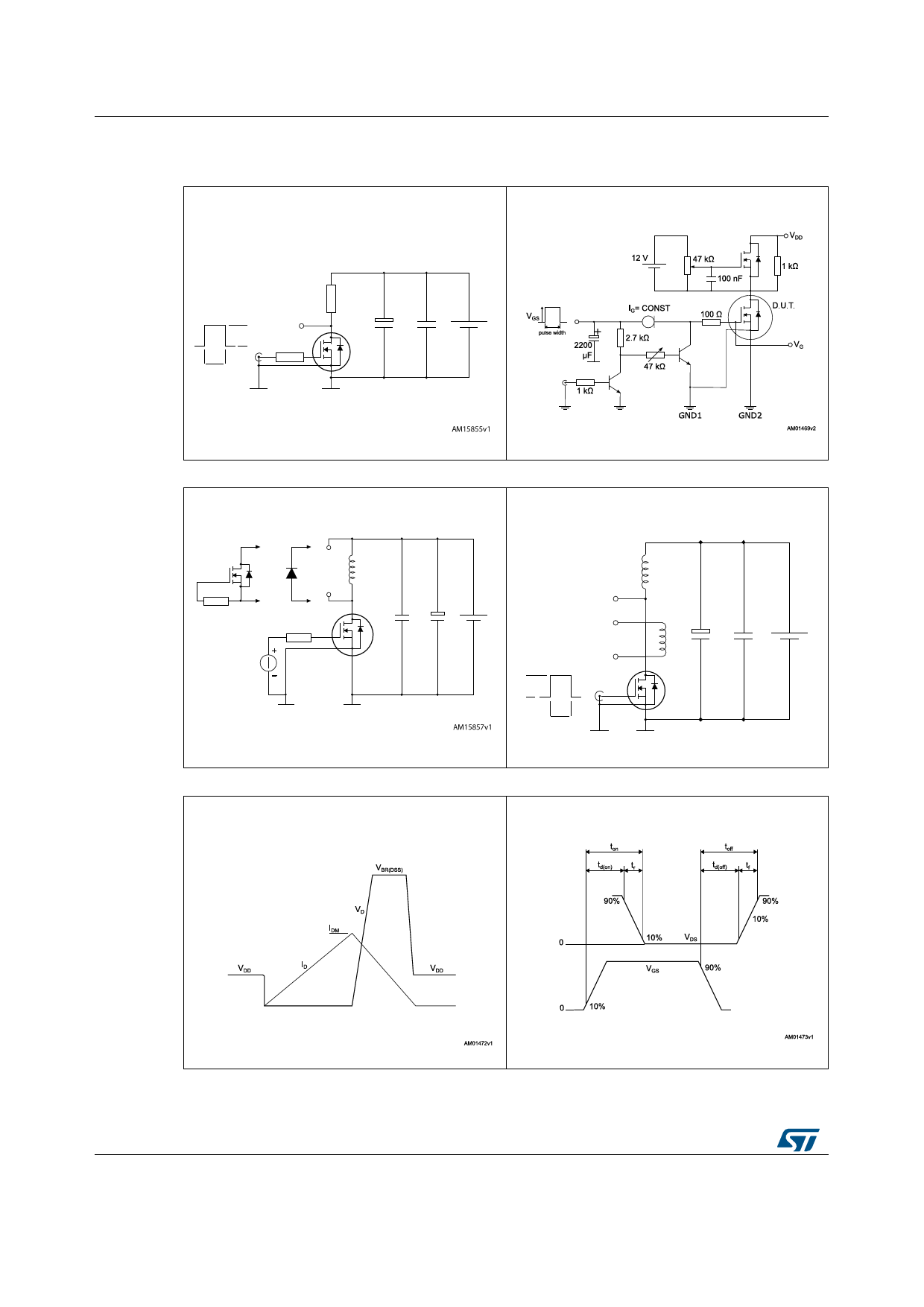
Test circuits
3
Test circuits
Figure 14: Switching times test circuit for
resistive load
STL24N60M2
Figure 15: Gate charge test circuit
VD
VGS
RG
PW
RL
2200
µF
+
D.U.T.
GND1
(driver signal)
GND2
(power)
3.3
µF VDD
Figure 16: Test circuit for inductive load
switching and diode recovery times
G
25Ω
A
D
D.U.T.
S
B
AA
FAST
DIODE
B
B
L=100µH
D
G
RG
S
D.U.T.
3.3
1000
µF + µF
VDD
GND1
GND2
Figure 17: Unclamped inductive load test
circuit
L
VD
2200
3.3
µF
µF
VDD
+
ID
Vi
D.U.T.
Pw
GND1
GND2
AM15858v1
Figure 18: Unclamped inductive waveform
Figure 19: Switching time waveform
8/15
DocID024777 Rev 3
Share Link: 