BA040LBSG 查看數據表(PDF) - ROHM Semiconductor
零件编号
产品描述 (功能)
生产厂家
BA040LBSG Datasheet PDF : 9 Pages
| |||
Regulator IC
BAΟΟΟLBSG Series
BA050LBSG (unless otherwise noted, Ta=25°C, VCC=6.0V)
Parameter
Symbol Min. Typ. Max. Unit
Coniditions
Standby current
Circuit current
ICCS
−
0
10
µA Vctl=0V
ICCa
−
65
150
µA Vctl=3V, no output load
<Output block>
Output voltage
Dropout voltage
VO
4.875 5.00 5.125
V Io=50mA∗1
∆Vd
−
90
150
mV Io=50mA, Vcc=0.95Vo
Output current capability
IO
150
280
−
mA
−
Load regulation
Reg.L
−
40
80
mV Io=1~50mA∗1
Input regulation
Output noise voltage
Reg.I
−
3
30
mV Vcc=6.0~7V
en
−
56
−
µV Io=10mA, C=0.01µF∗2
Ripple rejection 1
Ripple rejection 2
R.R1
45
54
−
dB Io=10mA, f=400Hz
R.R2
−
66
−
dB Io=10mA, f=400Hz, C=0.01µF∗2
<Power-save block>
CTL OFF voltage
Voff
−
−
0.6
V
−
CTL ON voltage
Von
2.4
−
−
V
−
CTL inflow current
Ictl
−
6.0
15
µA Vctl=3V
∗ In order to measure at Ta Tj (pulse measurement), fluctuations in output resulting from temperature fluctuations are not included.
∗ Design guaranteed. (Not all products have been inspected.)
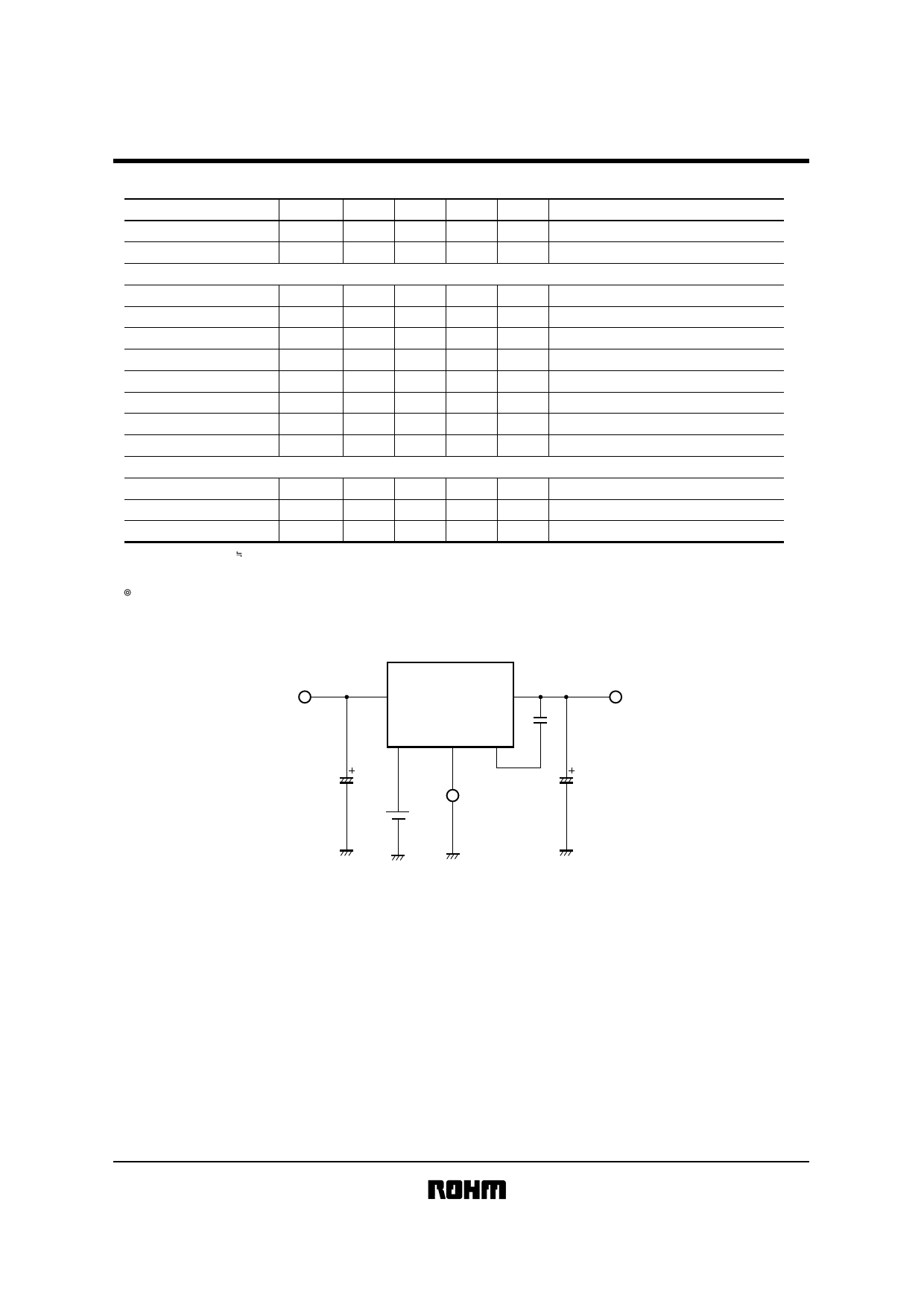
A capacitor (0.01µF) is used between pin 4 and pin 5, to improve ripple rejection.
Not designed for radiation resistance.
!Application example
0.01µF
VCC
OUT
CTL
GND
C
1µF
10µF
Fig.1
Share Link: 