NCV8508D2T50R4G(2009) 查看數據表(PDF) - ON Semiconductor
零件编号
产品描述 (功能)
生产厂家
NCV8508D2T50R4G Datasheet PDF : 26 Pages
| |||
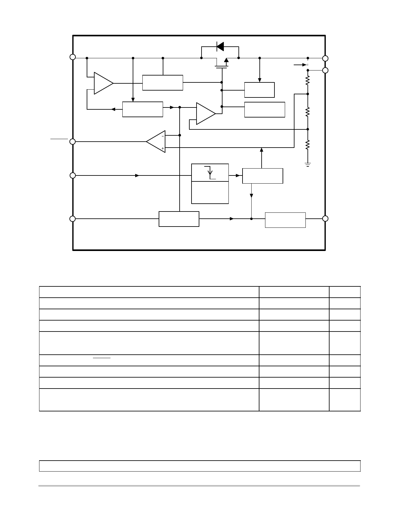
NCV8508
VIN
RESET
−
Charge
+
Pump
11 V
Bandgap
1.25 V
+
Reference
−
WDI
Delay
Timing
Circuit
Falling
Edge
Detect
Internally
connected
on 7 lead
D2PAK
Current
Limit
Thermal
Shutdown
Watchdog
Circuit
Wakeup
Circuit
VOUT
Sense
Wakeup
Figure 2. Block Diagram
MAXIMUM RATINGS
Rating
Value
Unit
Input Voltage, VIN (DC)
−0.3 to 45
V
Peak Transient Voltage (46 V Load Dump @ VIN = 14 V)
60
V
Output Voltage, VOUT
−0.3 to 18
V
ESD Susceptibility:
Human Body Model
2.0
kV
Machine Model
150
V
Logic Inputs/Outputs (RESET, WDI, Wakeup)
−0.3 to +7.0
V
Operating Junction Temperature, TJ
−40 to150
°C
Storage Temperature Range, TS
−55 to +150
°C
Peak Reflow Soldering Temperature:
Reflow: (Note 1)
240 Peak
°C
260 Peak (Pb−Free)
(Note 3)
Stresses exceeding Maximum Ratings may damage the device. Maximum Ratings are stress ratings only. Functional operation above the
Recommended Operating Conditions is not implied. Extended exposure to stresses above the Recommended Operating Conditions may affect
device reliability.
1. 60 second maximum above 183°C.
2. Depending on thermal properties of substrate RqJA = RqJC + RqJCA.
3. −5°C/+0°C allowable conditions, applies to both Pb and Pb−Free devices.
THERMAL CHARACTERISTICS
See Package Thermal Data Section (Page 10)
http://onsemi.com
3
Share Link: 