SQ6601PT 查看數據表(PDF) - AUK -> KODENSHI CORP
零件编号
产品描述 (功能)
生产厂家
SQ6601PT Datasheet PDF : 8 Pages
| |||
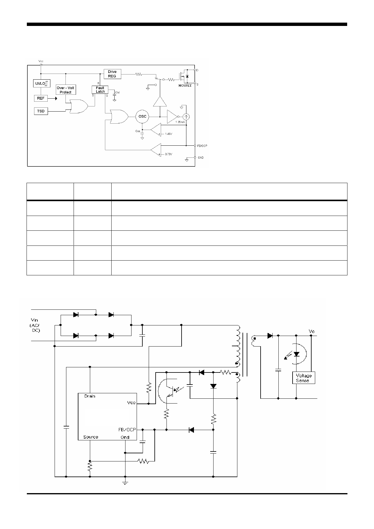
Internal Block Diagram
SQ6601PT
Pin Function
Pin Number Pin Name
Pin Function
1
Drain Power Switch MOSFET Drain Part
2
Source Power Switch MOSFET Source Part
3
GND Ground of the Control Section
4
Vcc
Supply Voltage of Output Drive & Control Section
5
FB/OCP Voltage Mode Control Feedback Signal & Over Current Detection
Typical Connection Diagram
SQ6601PT
KSD-I0U001-000
2
Share Link: 