UC2842A 查看數據表(PDF) - Motorola => Freescale
零件编号
产品描述 (功能)
生产厂家
UC2842A Datasheet PDF : 14 Pages
| |||
UC3842A, 43A UC2842A, 43A
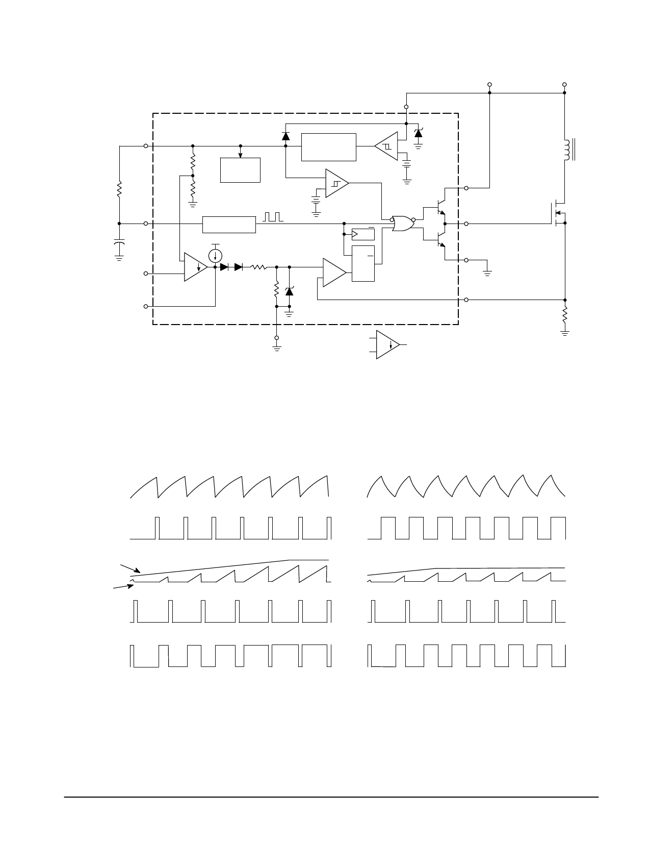
Figure 17. Representative Block Diagram
VCC
VCC 7(12)
Vref
8(14)
R
2.5V
RT
R
Internal
Bias
4(7)
CT
Voltage Feedback
Input
2(3)
Output
Compensation
1(1)
Oscillator
+
1.0mA
+
–
Error
Amplifier
2R
R
Reference
+
36V
Regulator
+
VCC – +
UVLO –
3.6V + – Vref
– UVLO
TQ
–
+
1.0V
Current Sense
Comparator
S
Q
R PWM
Latch
VC
7(11)
Output
6(10)
Power Ground
5(8)
Current Sense Input
3(5)
Gnd 5(9)
+
–
Pin numbers in parenthesis are for the D suffix SO–14 package.
=
Sink Only
Positive True Logic
Vin
Q1
RS
Capacitor CT
Latch
‘‘Set’’ Input
Output/
Compensation
Current Sense
Input
Latch
‘‘Reset’’ Input
Output
Figure 18. Timing Diagram
Large RT/Small CT
Small RT/Large CT
MOTOROLA ANALOG IC DEVICE DATA
7
Share Link: 