CS52843ED14 查看數據表(PDF) - Cherry semiconductor
零件编号
产品描述 (功能)
生产厂家
CS52843ED14 Datasheet PDF : 6 Pages
| |||
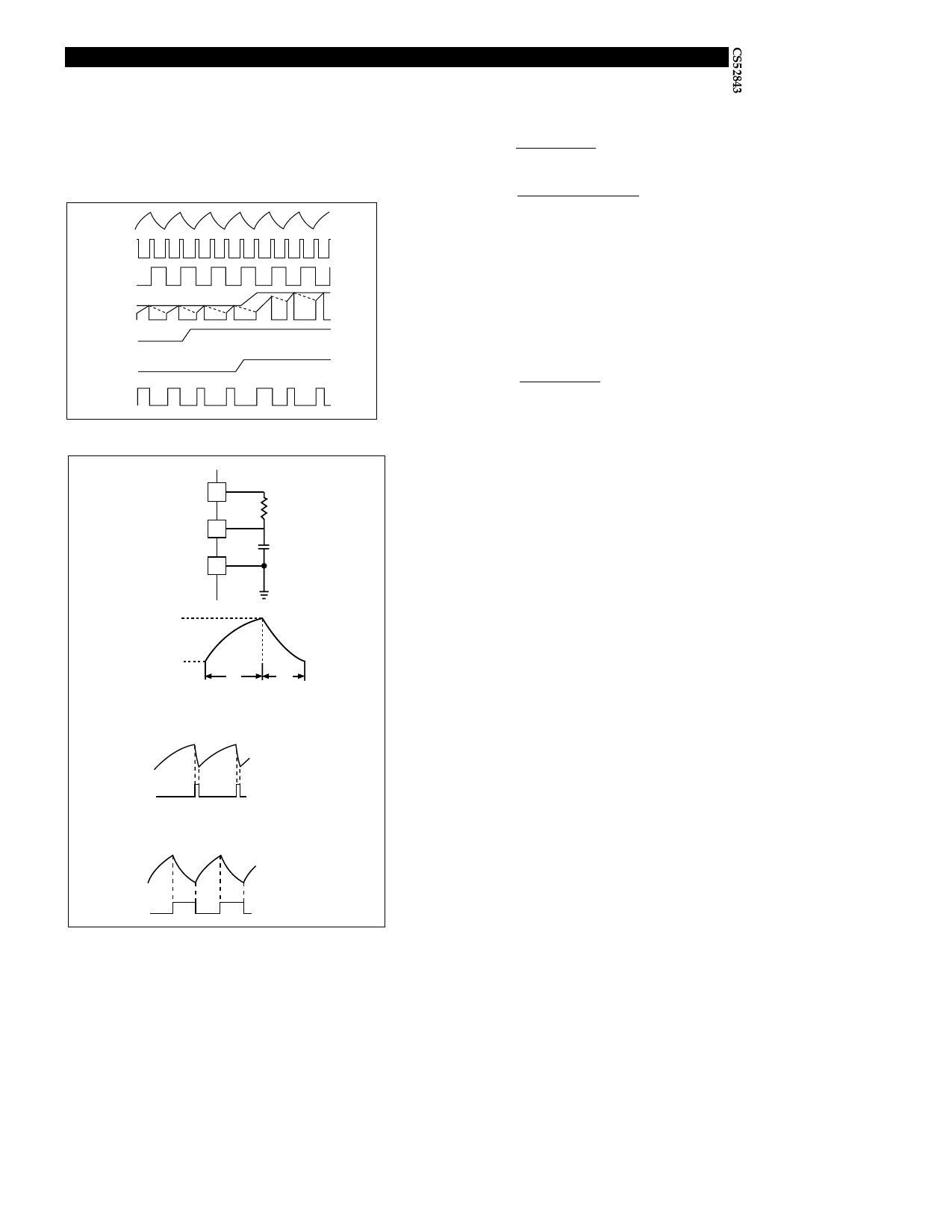
Circuit Description
When the power supply sees a sudden large output cur-
rent increase, the control voltage will increase allowing the
duty cycle to momentarily increase. Since the duty cycle
tends to exceed the maximum allowed to prevent trans-
former saturation in some power supplies, the internal
oscillator waveform provides the maximum duty cycle
clamp as programmed by the selection of oscillator timing
components.
VOSC
OSC
RESET
Toggle
F/F Output
EA Output
Switch
Current
VCC
Setting the Oscillator
The times Tc and Td can be determined as follows:
( ) tc = RTCT ln
VREF - VLOWER
VREF - VUPPER
( ) td = RTCT ln
VREF - IdRT - VLOWER
VREF - IdRT - VUPPER
Substituting in typical values for the parameters in the
above formulas:
VREF = 5.0V, VUPPER = 2.7V, VLOWER = 1.0V, Id = 8.3mA,
then
tc ≈ 0.5534RTCT
IO
VO
Figure 2: Timing Diagram
VREF
RT
OSC
CT
Gnd
( ) td = RTCT ln
2.3 - 0.0083 RT
4.0 - 0.0083 RT
For better accuracy RT should be ≥10kΩ.
Grounding
High peak currents associated with capacitive loads neces-
sitate careful grounding techniques. Timing and bypass
capacitors should be connected close to Gnd in a single
point ground.
The transistor and 5kΩ potentiometer are used to sample
the oscillator waveform and apply an adjustable ramp to
Sense.
Vupper
Vlower
tc
td
Sawtooth Mode
LARGE RT (≈10kΩ)
VOSC
Triangular Mode
SMALL RT (≈700kΩ)
Internal Clock
VREF
Internal Clock
Figure 3: Oscillator Timing Network and Parameters
5
Share Link: 