7N60F 查看數據表(PDF) - Unspecified
零件编号
产品描述 (功能)
生产厂家
7N60F Datasheet PDF : 9 Pages
| |||
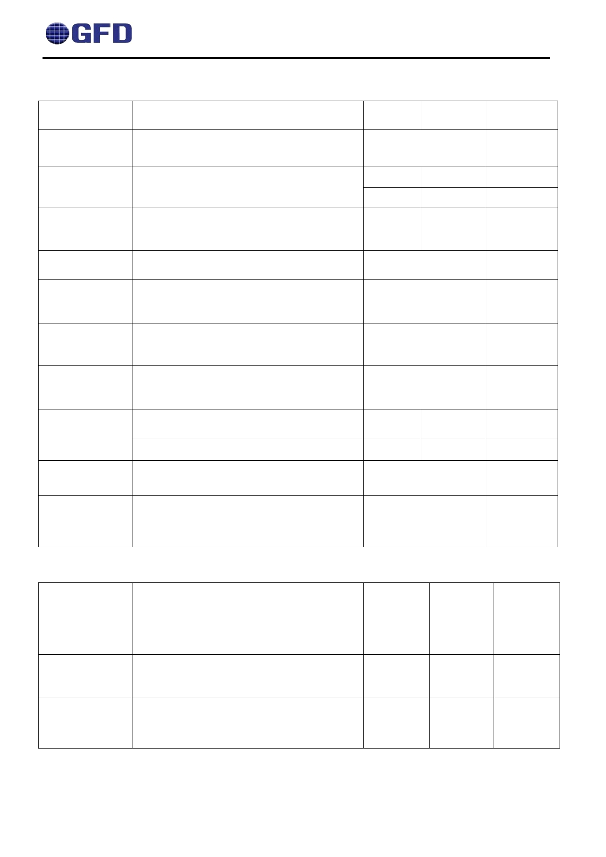
7N60/7N60F
Absolute Maximum Ratings
TC = 25°Cunless otherwise noted
Symbol
Parameter
7N60
7N60F
VDSS
ID
Drain-Source Voltage
Drain Current - Continuous (TC = 25°C)
- Continuous (TC = 100°C)
600
7.0
7.0
4.2
4.2
IDM
Drain Current- Pulsed
(Note 1)
28
28
VGSS
Gate-Source Voltage
± 30
EAS
Single Pulsed Avalanche Energy
(Note 2)
245
Units
V
A
A
A
V
mJ
EAR
Repetitive Avalanche Energy
(Note 1)
14.7
mJ
dv/dt
Peak Diode Recovery dv/dt
(Note 3)
4.5
V/ns
PD
TJ, TSTG
TL
Power Dissipation (TC = 25°C)
Derate above 25°C
Operating and Storage Temperature Range
Maximum lead temperature for soldering
purposes,
1/8" from case for 5 seconds
147
48
1.17
0.38
-55 to +150
300
W
W/°C
°C
°C
Thermal Characteristics
Symbol
Parameter
7N60
7N60F
Units
RθJC
Thermal Resistance, Junction-to-Case
0.85
2.6
°C/W
RθCS
Thermal Resistance, Case-to-Sink Typ.
0.5
--
°C/W
RθJA
Thermal Resistance, Junction-to-Ambient
62.5
62.5
°C/W
www.goford.cn TEL:0755-86350980 FAX:0755-86350963
Share Link: 