MAX9109EUT-T 查看數據表(PDF) - Maxim Integrated
零件编号
产品描述 (功能)
生产厂家
MAX9109EUT-T Datasheet PDF : 9 Pages
| |||
MAX9107/MAX9108/MAX9109
25ns, Dual/Quad/Single, Low-Power,
TTL Comparators
General Description
The MAX9107/MAX9108/MAX9109 dual/quad/single,
high-speed, low-power voltage comparators are designed
for use in systems powered from a single +5V supply.
Their 25ns propagation delay (with 10mV input overdrive)
is achieved with a power consumption of only 1.75mW
per comparator. The wide input common-mode range
extends from 200mV below ground to within 1.5V of the
positive supply rail.
The MAX9107/MAX9108/MAX9109 outputs are TTL-
compatible, requiring no external pullup circuitry. These
easy-to-use comparators incorporate internal hysteresis
to ensure clean output switching even when the devices
are driven by a slow-moving input signal.
The MAX9107/MAX9108/MAX9109 are higher-speed,
lower-power, lower-cost upgrades to industry-standard
comparators MAX907/MAX908/MAX909. The MAX9109
features an output latch but does not have complemen-
tary outputs.
The dual MAX9107 is available in both 8-pin SO and
SOT23 packages. The quad MAX9108 is available
in 14-pin TSSOP and SO packages while the single
MAX9109 is available in an ultra-small 6-pin SC70 pack-
age, a space-saving 6-pin SOT23 package and an 8-pin
SO package.
Applications
●● Battery Powered Systems ●● Threshold Detectors/
●● A/D Converters
Discriminators
●● Line Receivers
●● Sampling Circuits
●● Zero-Crossing Detectors
Features
●● 25ns Propagation Delay
●● 350µA (1.75mW) Supply Current Per Comparator
●● Single 4.5V to 5.5V Supply Operation
●● Wide Input Range Includes Ground
●● Low 500µV Offset Voltage
●● Internal Hysteresis Provides Clean Switching (2mV)
●● TTL-Compatible Outputs
●● Internal Latch (MAX9109 only)
●● Space-Saving Packages:
• 6-Pin SC70 (MAX9109)
• 8-Pin SOT23 (MAX9107)
• 14-Pin TSSOP (MAX9108)
Ordering Information
PART
PIN-
PACKAGE
TOP
MARK
PKG
CODE
MAX9107EKA+T
MAX9107ESA+
8 SOT23-8
8 SO
AAIB
—
K8-5
S8-2
MAX9108EUD+
14 TSSOP
—
U14-1
MAX9108ESD+
14 SO
—
S14-1
MAX9109EXT+T 6 SC70-6
AAU
X6S-1
MAX9109EUT+T 6 SOT23-6
AARU
U6-1
MAX9109ESA+
8 SO
—
S8-2
Note: All devices are specified over the -40°C to +85°C operat-
ing temperature range.
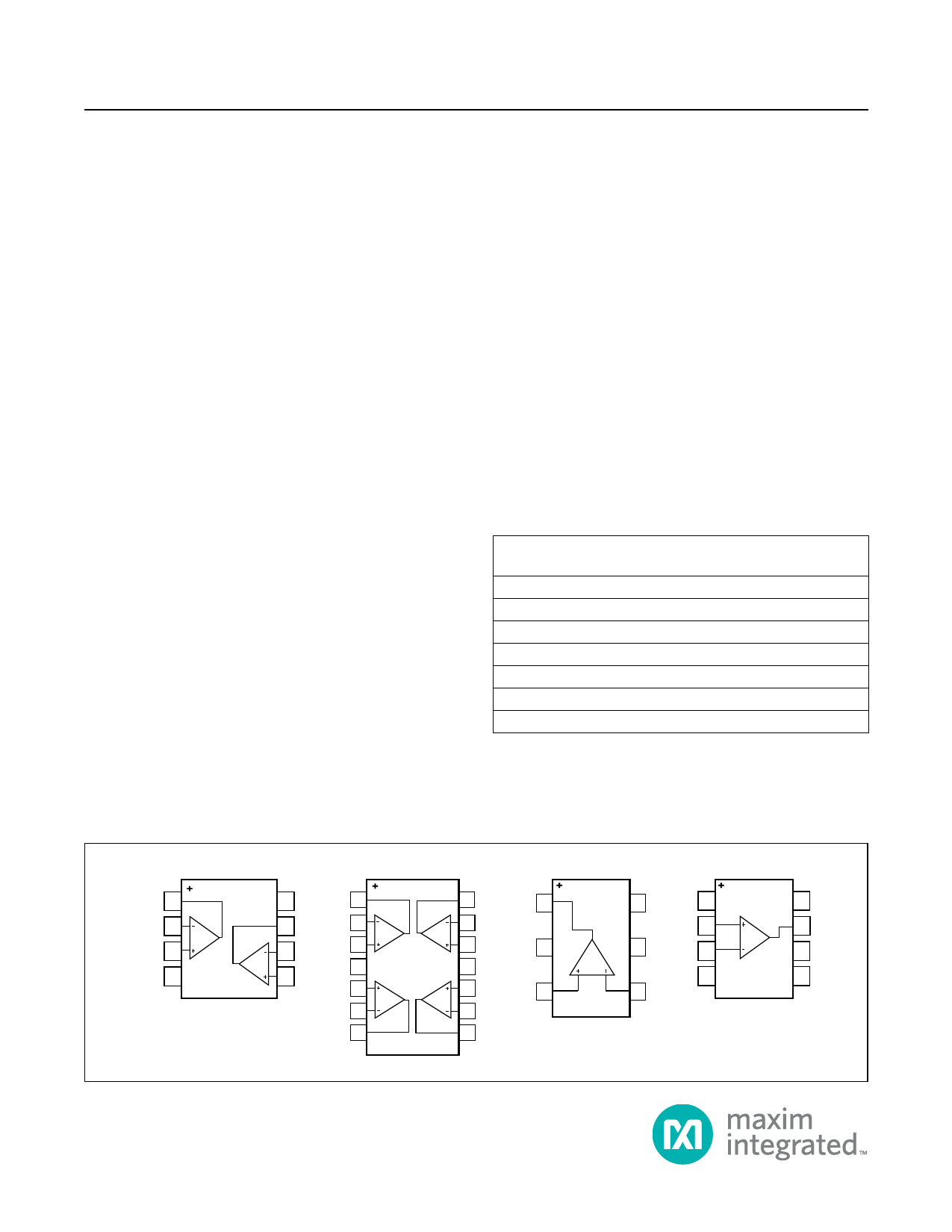
Pin Configurations
TOP VIEW
OUTA 1
INA- 2
INA+ 3
GND 4
MAX9107
SOT23/SO
8 VCC OUTA 1
7 OUTB INA- 2
6 INB- INA+ 3
5 INB+ VCC 4
INB+ 5
INB- 6
OUTB 7
A
D
MAX9108
B
C
MAX9109
14 OUTD OUT 1
6 VCC VCC 1 MAX9109
13 IND-
IN+ 2
12 IND+ GND 2
11 GND
10 INC+
9 INC-
IN+ 3
5 LE IN- 3
N.C. 4
4 IN-
SO
8 OUTC
SC70/SOT23
8 N.C.
7 OUT
6 GND
5 LE
TSSOP/SO
19-2045; Rev 3; 3/18
Share Link: 