530AA622M080DG 查看數據表(PDF) - Unspecified
零件编号
产品描述 (功能)
生产厂家
530AA622M080DG Datasheet PDF : 12 Pages
| |||
Si530/531
2. Pin Descriptions
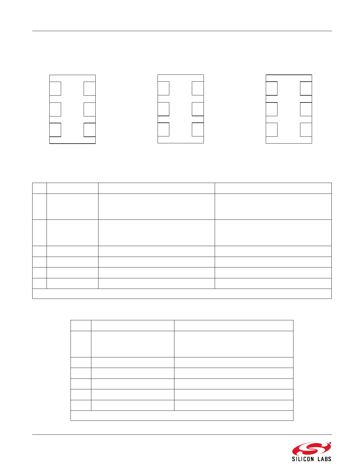
(Top View)
NC 1
6 VDD
OE 1
6 VDD
OE 1
6 VDD
OE 2
5 CLK–
NC 2
5 NC
NC 2
5 CLK–
GND 3
4 CLK+
GND 3
4 CLK
GND 3
4 CLK+
Si530
LVDS/LVPECL/CML
Si530
CMOS
Si531
LVDS/LVPECL/CML
Table 10. Pinout for Si530 Series
Pin
Symbol
LVDS/LVPECL/CML Function
CMOS Function
1 OE (CMOS only)*
No connection
Output enable
0 = clock output disabled (outputs tristated)
1 = clock output enabled
OE
Output enable
2 (LVPECL,LVDS, 0 = clock output disabled (outputs tristated)
CML)*
1 = clock output enabled
No connection
3
GND
Electrical and Case Ground
Electrical and Case Ground
4
CLK+
Oscillator Output
Oscillator Output
5
CLK–
Complementary Output
No connection
6
VDD
Power Supply Voltage
*Note: OE includes a 17 k pullup resistor to VDD.
Power Supply Voltage
Table 11. Pinout for Si531 Series
Pin
Symbol
LVDS/LVPECL/CML Function
Output enable
1 OE (LVPECL, LVDS, CML)* 0 = clock output disabled (outputs tristated)
1 = clock output enabled
2
No connection
No connection
3
GND
Electrical and Case Ground
4
CLK+
Oscillator Output
5
CLK–
Complementary output
6
VDD
*Note: OE includes a 17 k pullup resistor to VDD.
Power Supply Voltage
6
Rev. 1.5
Share Link: 