MAX6709 وں¥çœ‹و•¸و“ڑè،¨ï¼ˆPDF) - Maxim Integrated
零ن»¶ç¼–هڈ·
ن؛§ه“پوڈڈè؟° (هٹں能)
ç”ںن؛§هژ‚ه®¶
MAX6709 Datasheet PDF : 13 Pages
| |||
Low-Voltage, High-Accuracy, Quad Voltage
Monitors in آµMAX Package
ABSOLUTE MAXIMUM RATINGS
All Pins to GND.........................................................-0.3V to +6V
Input/Output Current (all pins) ............................................20mA
Continuous Power Dissipation (TA = +70آ°C)
10-Pin آµMAX (derate 5.6mW/آ°C above +70آ°C) ..........444mW
Operating Temperature Range ...........................-40آ°C to +85آ°C
Storage Temperature Range .............................-65آ°C to +150آ°C
Junction Temperature ......................................................+150آ°C
Lead Temperature (soldering, 10s) .................................+300آ°C
Stresses beyond those listed under “Absolute Maximum Ratings†may cause permanent damage to the device. These are stress ratings only, and functional
operation of the device at these or any other conditions beyond those indicated in the operational sections of the specifications is not implied. Exposure to
absolute maximum rating conditions for extended periods may affect device reliability.
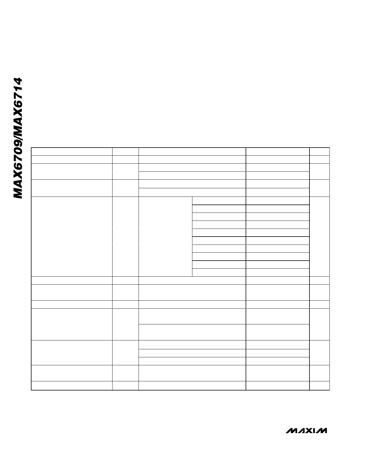
ELECTRICAL CHARACTERISTICS (MAX6709)
(VCC = 2.0V to 5.5V, TA = -40آ°C to +85آ°C, unless otherwise noted. Typical values are at VCC = 5V and TA = +25آ°C.) (Note 1)
PARAMETER
Supply Voltage Range
Supply Current
Input Current
Threshold Voltage
Adjustable Threshold
Threshold Voltage Temperature
Coefficient
SYMBOL
VCC
ICC
IIN_
VTH
VTH
CONDITIONS
VCC = 3V
VCC = 5V
VIN_ = input threshold voltage
VIN_ = 0 to 0.85V (for adjustable threshold)
5.0V (-5%)
5.0V (-10%)
3.3V (-5%)
3.3V (-10%)
IN_ decreasing
3.0V (-5%)
3.0V (-10%)
2.5V (-5%)
2.5V (-10%)
1.8V (-5%)
1.8V (-10%)
IN_ decreasing
TCVTH
MIN
2.0
4.50
4.25
3.00
2.85
2.70
2.55
2.25
2.13
1.62
1.53
0.609
TYP
25
35
25
4.63
4.38
3.08
2.93
2.78
2.63
2.32
2.19
1.67
1.58
0.623
MAX
5.5
50
65
40
0.2
4.75
4.50
3.15
3.00
2.85
2.70
2.38
2.25
1.71
1.62
0.635
UNITS
V
آµA
آµA
V
V
60
ppm/آ°C
Threshold Hysteresis
Propagation Delay
VHYST
tPD
VIN_ falling at 10mV/آµs from
VTH to (VTH - 50mV)
VIN_ rising at 10mV/آµs from
VTH to (VTH + 50mV)
0.3 x VTH
%
30
آµs
5
Output Low Voltage
Output High Voltage
VCC = 5V, ISINK = 2mA
VOL
VCC = 2.5V, ISINK = 1.2mA
VCC = 1V, ISINK = 50آµA (Note 2)
VCC ≥ 2.0V, ISOURCE = 6آµA (min), PWRGD_
VOH
unasserted
0.8 x VCC
0.3
0.3
V
0.3
V
Output High Source Current
IOH
VCC ≥ 2.0V, PWRGD_ unasserted
10
آµA
2 _______________________________________________________________________________________
Share Link: 