74VHC86 查看數據表(PDF) - STMicroelectronics
零件编号
产品描述 (功能)
生产厂家
74VHC86 Datasheet PDF : 8 Pages
| |||
74VHC86
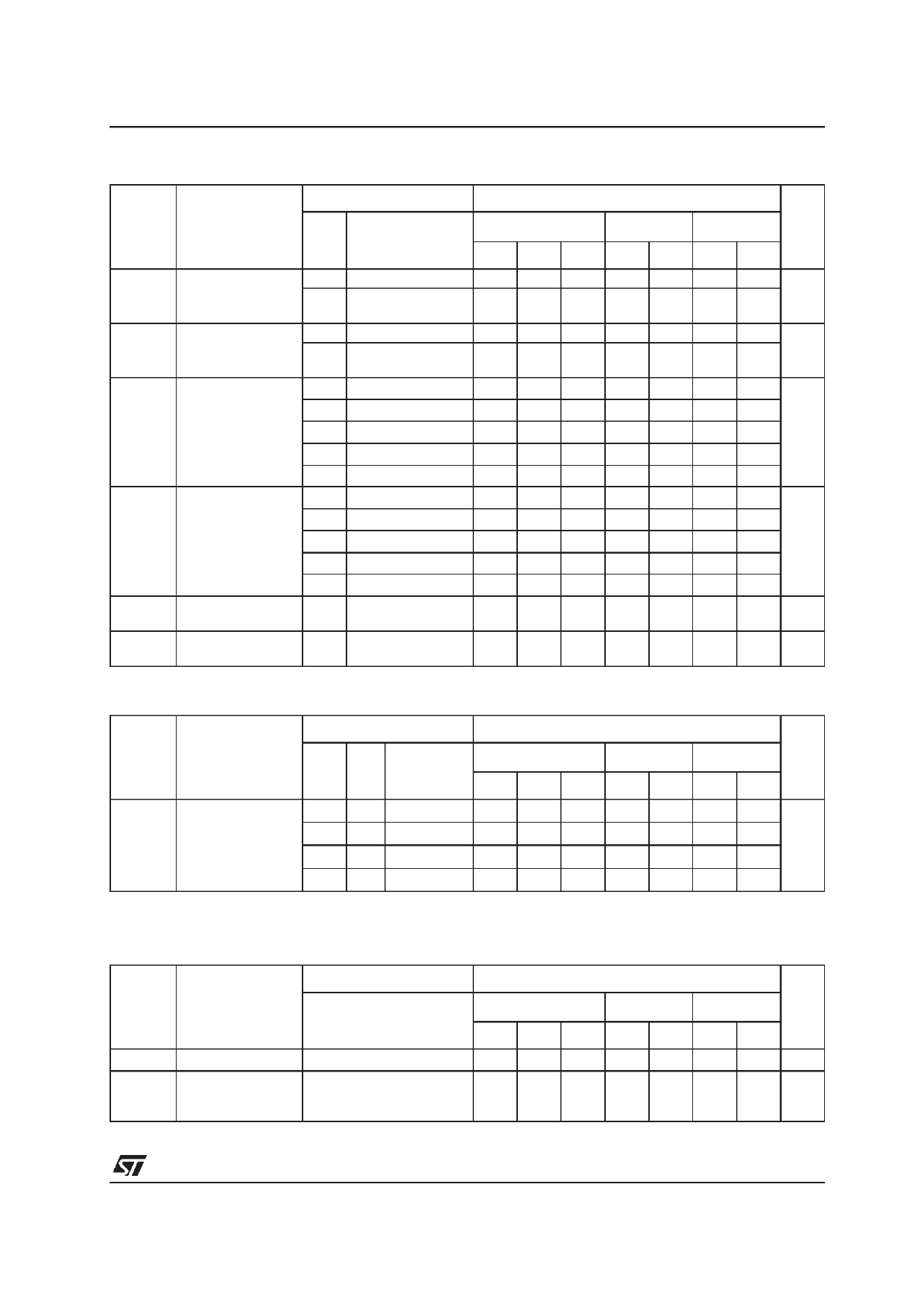
DC SPECIFICATIONS
Test Condition
Value
Symbol
Parameter
VIH High Level Input
Voltage
VIL Low Level Input
Voltage
VOH High Level Output
Voltage
VOL Low Level Output
Voltage
II
Input Leakage
Current
ICC Quiescent Supply
Current
VCC
(V)
2.0
3.0 to
5.5
2.0
3.0 to
5.5
2.0
3.0
4.5
3.0
4.5
2.0
3.0
4.5
3.0
4.5
0 to
5.5
5.5
TA = 25°C
-40 to 85°C -55 to 125°C Unit
Min. Typ. Max. Min. Max. Min. Max.
1.5
0.7VCC
1.5
1.5
V
0.7VCC
0.7VCC
0.5
0.3VCC
0.5
0.3VCC
0.5
V
0.3VCC
IO=-50 µA
IO=-50 µA
IO=-50 µA
IO=-4 mA
IO=-8 mA
IO=50 µA
IO=50 µA
IO=50 µA
IO=4 mA
IO=8 mA
1.9 2.0
1.9
1.9
2.9 3.0
2.9
2.9
4.4 4.5
4.4
4.4
V
2.58
2.48
2.4
3.94
3.8
3.7
0.0 0.1
0.1
0.1
0.0 0.1
0.1
0.1
0.0 0.1
0.1
0.1 V
0.36
0.44
0.55
0.36
0.44
0.55
VI = 5.5V or GND
± 0.1
±1
± 1 µA
VI = VCC or GND
2
20
20 µA
AC ELECTRICAL CHARACTERISTICS (Input tr = tf = 3ns)
Test Condition
Value
Symbol
Parameter
VCC CL
(V) (pF)
tPLH Propagation Delay 3.3(*) 15
tPHL Time
3.3(*) 50
5.0(**) 15
5.0(**) 50
(*) Voltage range is 3.3V ± 0.3V
(**) Voltage range is 5.0V ± 0.5V
TA = 25°C
-40 to 85°C -55 to 125°C Unit
Min. Typ. Max. Min. Max. Min. Max.
7.0 11.0 1.0 13.0 1.0 13.0
9.5 14.5 1.0 16.5 1.0 16.5
ns
4.8 6.8 1.0 8.0 1.0 8.0
6.3 8.8 1.0 10.0 1.0 10.0
CAPACITIVE CHARACTERISTICS
Test Condition
Value
Symbol
Parameter
TA = 25°C
-40 to 85°C -55 to 125°C Unit
Min. Typ. Max. Min. Max. Min. Max.
CIN Input Capacitance
6 10
10
10 pF
CPD Power Dissipation
Capacitance
18
pF
(note 1)
1) CPD is defined as the value of the IC’s internal equivalent capacitance which is calculated from the operating current consumption without
load. (Refer to Test Circuit). Average operating current can be obtained by the following equation. ICC(opr) = CPD x VCC x fIN + ICC/4 (per gate)
3/8
Share Link: 