AD5425 查看數據表(PDF) - Analog Devices
零件编号
产品描述 (功能)
生产厂家
AD5425 Datasheet PDF : 24 Pages
| |||
Data Sheet
AD5425
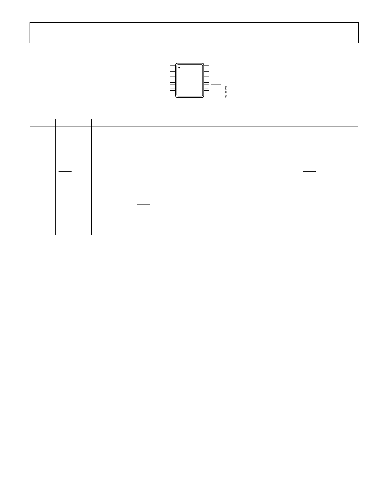
PIN CONFIGURATION AND FUNCTION DESCRIPTIONS
IOUT1 1
IOUT2 2
GND 3
SCLK 4
SDIN 5
AD5425
TOP VIEW
(Not to Scale)
10 RFB
9 VREF
8 VDD
7 LDAC
6 SYNC
Figure 3. Pin Configuration
Table 4. Pin Function Descriptions
Pin No. Mnemonic Function
1
IOUT1
DAC Current Output.
2
IOUT2
DAC Analog Ground. This pin must normally be tied to the analog ground of the system.
3
GND
Digital Ground Pin.
4
SCLK
Serial Clock Input. Data is clocked into the input shift register on each falling edge of the serial clock input.
This device can accommodate clock rates of up to 50 MHz.
5
SDIN
Serial Data Input. Data is clocked into the 8-bit input register on each falling edge of the serial clock input.
6
SYNC
Active Low Control Input. This is the frame synchronization signal for the input data. When SYNC goes low, it
powers on the SCLK and DIN buffers and the input shift register is enabled. Data is transferred on each falling
edge of the following 8 clocks.
7
LDAC
Load DAC Input. Updates the DAC output. The DAC is updated when this signal goes low or alternatively; if this
line is held permanently low, an automatic update mode is selected whereby the DAC is updated after 8 SCLK
falling edges with SYNC low.
8
VDD
Positive Power Supply Input. This device can be operated from a supply of 2.5 V to 5.5 V.
9
VREF
DAC Reference Voltage Input Terminal.
10
RFB
DAC Feedback Resistor Pin. Establishes voltage output for the DAC by connecting to external amplifier output.
Rev. D | Page 7 of 24
Share Link: 