MPSA63 查看數據表(PDF) - Motorola => Freescale
零件编号
产品描述 (功能)
生产厂家
MPSA63 Datasheet PDF : 4 Pages
| |||
MOTOROLA
SEMICONDUCTOR TECHNICAL DATA
Darlington Transistors
PNP Silicon
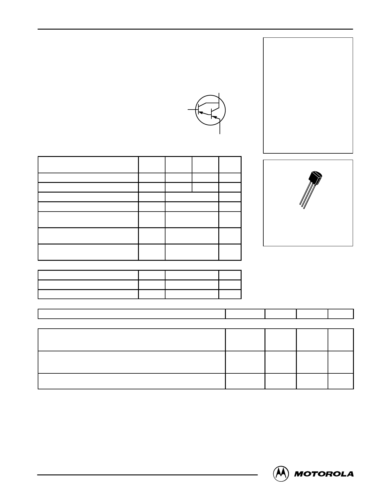
COLLECTOR 3
BASE
2
EMITTER 1
MAXIMUM RATINGS
Rating
MPSA63
Symbol MPSA62 MPSA64 Unit
Collector – Emitter Voltage
Collector – Base Voltage
Emitter – Base Voltage
Collector Current — Continuous
Total Device Dissipation @ TA = 25°C
Derate above 25°C
VCES
VCBO
VEBO
IC
PD
–20
–30
–20
–30
–10
–500
625
5.0
Vdc
Vdc
Vdc
mAdc
mW
mW/°C
Total Device Dissipation @ TA = 25°C
PD
Derate above 25°C
1.5
Watts
12
mW/°C
Operating and Storage Junction
Temperature Range
TJ, Tstg
– 55 to +150
°C
THERMAL CHARACTERISTICS
Characteristic
Symbol
Max
Unit
Thermal Resistance, Junction to Ambient RqJA
200
Thermal Resistance, Junction to Case
RqJC
83.3
ELECTRICAL CHARACTERISTICS (TA = 25°C unless otherwise noted)
Characteristic
°C/W
°C/W
Symbol
OFF CHARACTERISTICS
Collector – Emitter Breakdown Voltage
(IC = –100 µAdc, VBE = 0)
MPSA62
MPSA63, MPSA64
V(BR)CES
Collector Cutoff Current
(VCB= –15 Vdc, IE = 0)
(VCB = –30 Vdc, IE = 0)
Emitter Cutoff Current
(VEB = –10 Vdc, IC = 0)
MPSA62
MPSA63, MPSA64
ICBO
IEBO
Order this document
by MPSA62/D
MPSA62
thru
MPSA64 *
MPSA55, MPSA56
For Specifications,
See MPSA05, MPSA06 Data
*Motorola Preferred Device
1
2
3
CASE 29–04, STYLE 1
TO–92 (TO–226AA)
Min
Max
Unit
Vdc
–20
—
–30
—
nAdc
—
–100
—
–100
—
–100
nAdc
Preferred devices are Motorola recommended choices for future use and best overall value.
©MMotootorroollaa,
Small–Signal
Inc. 1996
Transistors,
FETs
and
Diodes
Device
Data
1
Share Link: 