SFH6315 查看數據表(PDF) - Infineon Technologies
零件编号
产品描述 (功能)
生产厂家
SFH6315 Datasheet PDF : 5 Pages
| |||
Switching Specifications
Over recommended temperature (TA=0°C to 70°C), VCC=5.0 V, IF=16 mA unless otherwise specified. *All typical values, TA=25°C
Parameter
Symbol Device Min. Typ.* Max. Units Test Conditions
Fig. Note
Propagation Delay Time
tPHL
to Logic Low at Output
SFH6315 — 0.5 1.5
2.0
µs
SFH6316 —
SFH6343
0.25 0.8
1.0
TA=25°C
TA=25°C
RL=4.1 kΩ
RL=1.9 kΩ
1 4, 5
Propagation Delay Time
to Logic High at Output
tPLH
SFH6315 — 0.5 1.5
2.0
µs
SFH6316 — 0.5 0.8
SFH6343
1.0
TA=25°C
TA=25°C
RL=4.1 kΩ
RL=1.9 kΩ
1 4, 5
Common Mode Transient
|CMH|
SFH6315 — 1.0
—
Immunity at Logic High
Level Output
SFH6316 — 1.0 —
SFH6343 15 30
—
kV/µs
RL=4.1 kΩ
RL=1.9 kΩ
RL=1.9 kΩ
IF=0 mA
TA=25°C
VCM=10 VP–P
2
IF=0 mA
TA=25°C
VCM=1500 VP–P
3, 4, 5
Common Mode Transient
|CML|
Immunity at Logic Low Level
Output
SFH6315 — 1.0 —
SFH6316 — 1.0 —
SFH6343 15 30
—
kV/µs
RL=4.1 kΩ
RL=1.9 kΩ
RL=1.9 kΩ
IF=16 mA
TA=25°C
VCM=10 VP–P
2
IF=16 mA
TA=25°C
VCM=1500 VP–P
3, 4, 5
Notes
1. Current transfer ratio in percent equals the ratio of output collector current (IO) to the forward LED input current (IF) times 100.
2. Device considered a two-terminal device: pins 1, 2, 3, and 4 shorted together and pins 5, 6, 7, and 8 shorted together.
3. Common mode transient immunity in a Logic High level is the maximum tolerable (positive) dVcm/dt on the leading edge of the common mode
pulse (VCM) to assure that the output will remain in a Logic High state (i.e., VO>2.0 V). Common mode transient immunity in a Logic Low level is
the maximum tolerable (negative) dVcm/dt on the trailing edge of the common mode pulse signal (VCM to assure that the output will remain in a
Logic Low state, i.e., VO<0.8 V).
4. The 1.9 kΩ load represents 1 TTL unit load of 1.6 mA and the 5.6 kΩ pull-up resistor.
5. The 4.1 kΩ load represents 1 LSTTL unit load of 0.36 mA and the 6.1 kΩ pull-up resistor.
6. A 0.1 µf bypass capacitor connected between pins 5 and 8 is recommended.
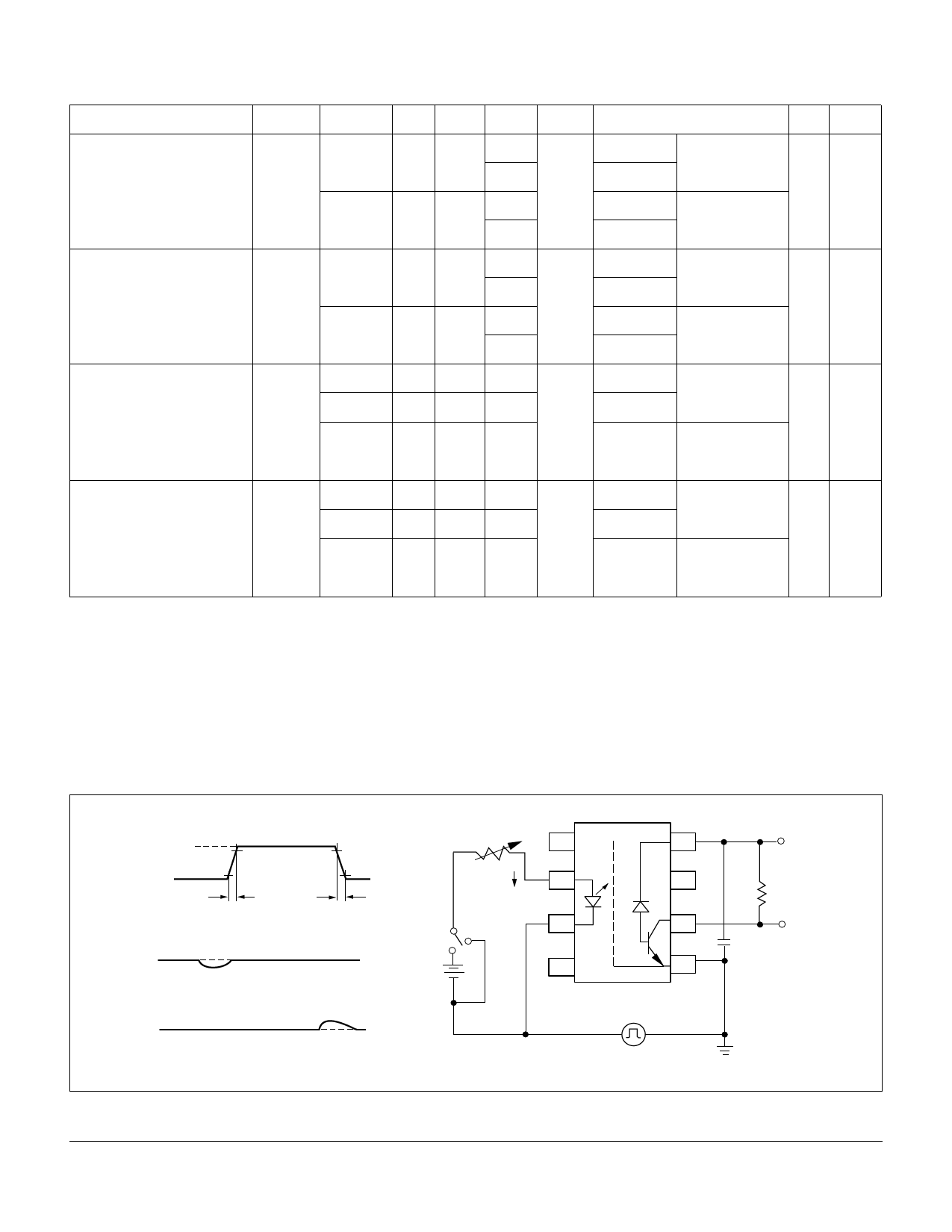
Figure 2. Test circuit for transient immunity and typical waveforms
VCM
0 V 10%
90%
tr
90%
10%
tf
1
8
IF
2
7
A
3
6
VO
B
5V
4
5
Switch at A: IF=0 mA
VCC
VO
VOL
Switch at B: IF=16 mA
VCM
+–
Pulse Generator
+5 V
RL
VO
0.1 µF
2000 Infineon Technologies Corp. • Optoelectronics Division • San Jose, CA
www.infineon.com/opto • 1-888-Infineon (1-888-463-4636)
OSRAM Opto Semiconductors GmbH & Co. OHG • Regensburg, Germany
www.osram-os.com • +49-941-202-7178
3
SFH6315/6316/6343
May 17, 2000–09
Share Link: 