HIP6007CB 查看數據表(PDF) - Renesas Electronics
零件编号
产品描述 (功能)
生产厂家
HIP6007CB Datasheet PDF : 10 Pages
| |||
HIP6007
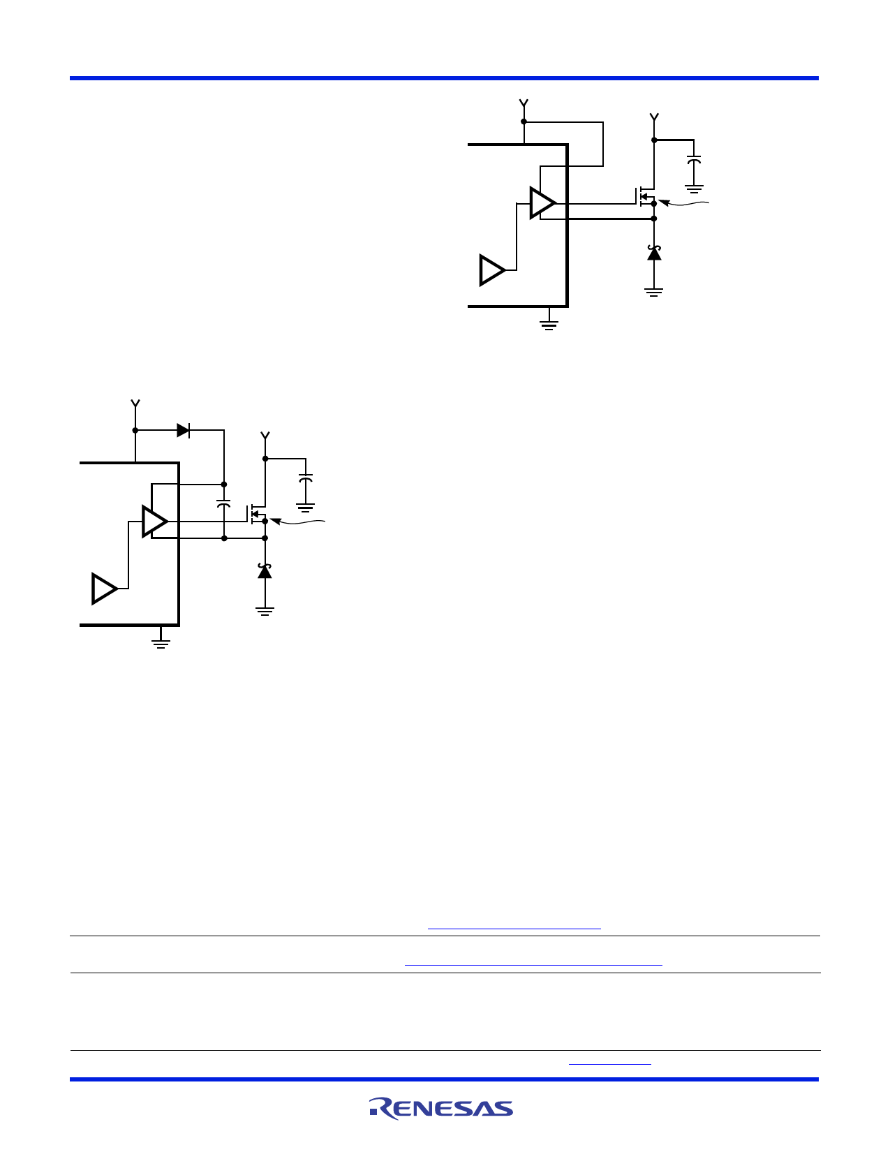
Figure 9 shows the upper gate drive (BOOT pin) supplied by a
bootstrap circuit from VCC. The boot capacitor, CBOOT
develops a floating supply voltage referenced to the PHASE
pin. This supply is refreshed each cycle to a voltage of VCC
less the boot diode drop (VD) when the lower MOSFET, Q2
turns on. A logic-level MOSFET can only be used for Q1 if the
MOSFET’s absolute gate-to-source voltage rating exceeds the
maximum voltage applied to VCC.
Figure 10 shows the upper gate drive supplied by a direct
connection to VCC. This option should only be used in
converter systems where the main input voltage is +5VDC or
less. The peak upper gate-to-source voltage is approximately
VCC less the input supply. For +5V main power and +12VDC
for the bias, the gate-to-source voltage of Q1 is 7V. A logic-
level MOSFET is a good choice for Q1 and a logic-level
MOSFET is a good choice for Q1 under these conditions.
+12V
DBOOT
VCC + VD -
+5V OR +12V
HIP6007
BOOT
CBOOT Q1
UGATE
PHASE
NOTE:
VG-S VCC - VD
D2
-
+
GND
FIGURE 9. UPPER GATE DRIVE - BOOTSTRAP OPTION
+12V
VCC
HIP6007
BOOT
UGATE
PHASE
-
+
+5V OR LESS
Q1
NOTE:
VG-S VCC - 5V
D2
GND
FIGURE 10. UPPER GATE DRIVE - DIRECT VCC DRIVE OPTION
Schottky Selection
Rectifier D2 conducts when the upper MOSFET Q1 is off. The
diode should be a Schottky type for low power losses. The
power dissipation in the schottky rectifier is approximated by:
PCOND = IO x Vf x (1 - D)
Where: D is the duty cycle = VO/VIN, and
Vf is the schottky forward voltage drop
In addition to power dissipation, package selection and heatsink
requirements are the main design tradeoffs in choosing the
schottky rectifier. Since the three factors are interrelated, the
selection process is an iterative procedure. The maximum
junction temperature of the rectifier must remain below the
manufacturer’s specified value, typically 125oC. By using the
package thermal resistance specification and the schottky
power dissipation equation (shown above), the junction
temperature of the rectifier can be estimated. Be sure to use the
available airflow and ambient temperature to determine the
junction temperature rise.
© Copyright Intersil Americas LLC 1997-2002. All Rights Reserved.
All trademarks and registered trademarks are the property of their respective owners.
For additional products, see www.intersil.com/en/products.html
Intersil products are manufactured, assembled and tested utilizing ISO9001 quality systems as noted
in the quality certifications found at www.intersil.com/en/support/qualandreliability.html
Intersil products are sold by description only. Intersil may modify the circuit design and/or specifications of products at any time without notice, provided that such
modification does not, in Intersil's sole judgment, affect the form, fit or function of the product. Accordingly, the reader is cautioned to verify that datasheets are
current before placing orders. Information furnished by Intersil is believed to be accurate and reliable. However, no responsibility is assumed by Intersil or its
subsidiaries for its use; nor for any infringements of patents or other rights of third parties which may result from its use. No license is granted by implication or
otherwise under any patent or patent rights of Intersil or its subsidiaries.
For information regarding Intersil Corporation and its products, see www.intersil.com
FN4307 Rev.1.00
September 1997
Page 9 of 10
Share Link: 