ISL62392 查看數據表(PDF) - Renesas Electronics
零件编号
产品描述 (功能)
生产厂家
ISL62392
Renesas Electronics
ISL62392 Datasheet PDF : 22 Pages
| |||
ISL62391, ISL62392, ISL62391C, ISL62392C
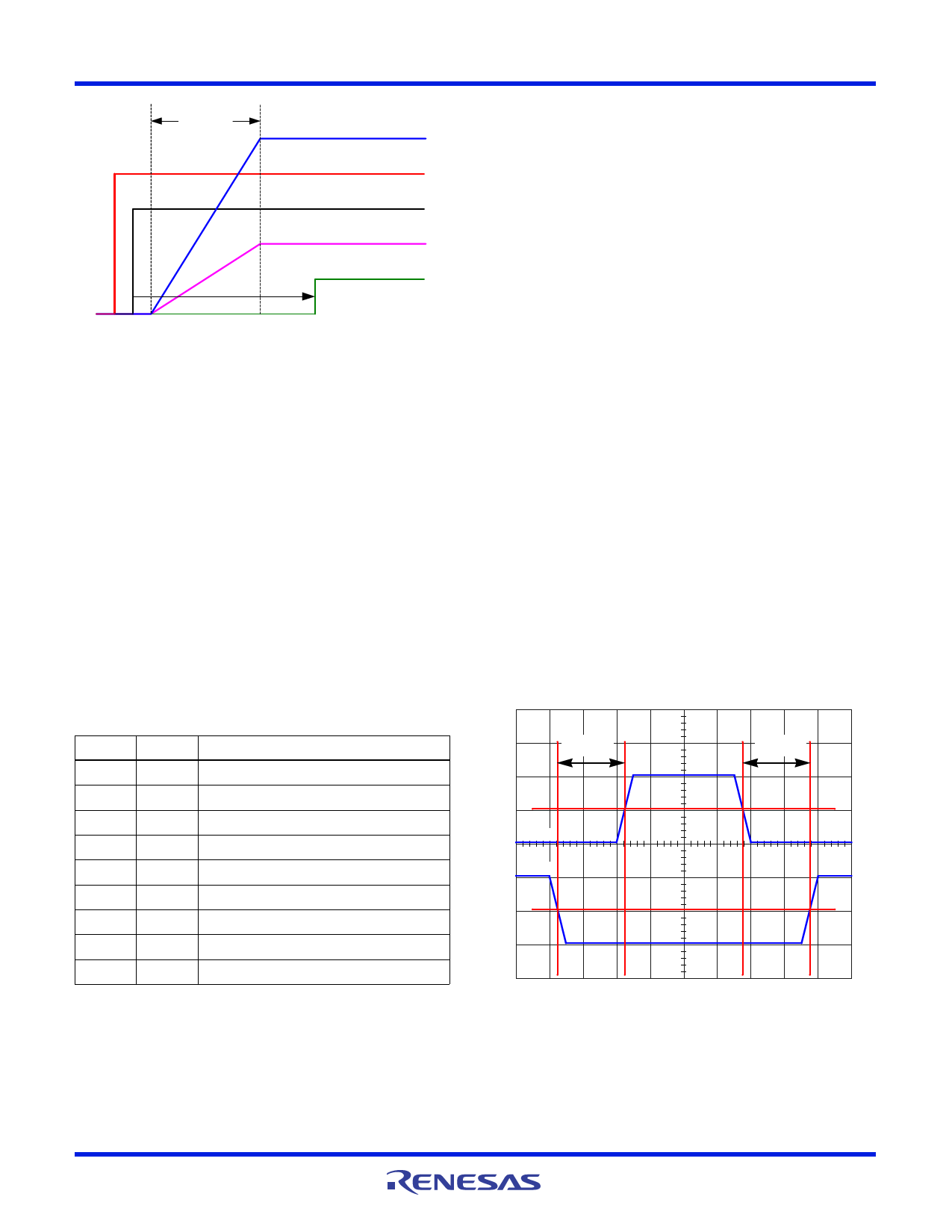
tS1O.5FTmSTsART
VO
VCC AND PVCC
EN
FB
2.75ms
PGOOD DELAY
PGOOD
FIGURE 24. SOFT-START SEQUENCE FOR ONE SMPS
The PGOOD pin indicates when the converter is capable of
supplying regulated voltage. It is an undefined impedance if VIN
is not above the rising POR threshold or below the POR falling
threshold. When a fault is detected, the ISL62391, ISL62392,
ISL62391C and ISL62392C will turn on the open-drain NMOS,
which will pull PGOOD low with a nominal impedance of 32
This will flag the system that one of the output voltages is out of
regulation.
Separate enable pins allow for full soft-start sequencing.
Because low shutdown quiescent current is necessary to
prolong battery life in notebook applications, the PVCC 5V LDO
is held off until any of the three enable signals (EN1, EN2 or
LDO3EN) are pulled high. Soft-start of all outputs will only start
until after PVCC is above the 4.2V POR threshold. In addition to
user-programmable sequencing, the ISL62391, ISL62392,
ISL62391C and ISL62392C include a pre-programmed
sequential SMPS soft-start feature. Table 1 shows the SMPS
enable truth table.
TABLE 1. SMPS ENABLE SEQUENCE LOGIC
EN1
EN2
START-UP SEQUENCE
0
0 All SMPS outputs OFF
0
FLOAT All SMPS outputs OFF
0
1 SMPS1 OFF, SMPS2 ON
FLOAT
0 All SMPS outputs OFF
FLOAT FLOAT All SMPS outputs OFF
FLOAT
1 SMPS1 enables after SMPS2 is in regulation
1
0 SMPS1 ON, SMPS2 OFF
1
FLOAT SMPS2 enables after SMPS1 is in regulation
1
1 All SMPS outputs ON simultaneously
VCC
The VCC nominal operation voltage is 5V. If EN1, EN2 and
LDO3EN are all logic low, the VCC start-up voltage is 3.6V
when VIN is applied on ISL62391, ISL62392, ISL62391C and
ISL62392C. PVCC is held off until any of the three enable
signals (EN1, EN2 or LDO3EN) is pulled high. When PVCC is
above the 4.2V VCC POR threshold, VCC will switchover to
PVCC internally.
After VIN is applied, the VCC start-up 3.6V voltage can be used
as the logic high signal of any of EN1, EN2 and LDO3EN to
enable PVCC if there is no other power supply on the board.
MOSFET Gate-Drive Outputs LGATE and UGATE
The ISL62391, ISL62392, ISL62391C and ISL62392C have
internal gate-drivers for the high-side and low-side N-Channel
MOSFETs. The low-side gate-drivers are optimized for low
duty-cycle applications where the low-side MOSFET
conduction losses are dominant, requiring a low r DS(ON)
MOSFET. The LGATE pull-down resistance is small in order to
clamp the gate of the MOSFET below the VGS(th) at turn-off. The
current transient through the gate at turn-off can be considerable
because the gate charge of a low r DS(ON) MOSFET can be large.
Adaptive shoot-through protection prevents a gate-driver output
from turning on until the opposite gate-driver output has fallen
below approximately 1V. The dead-time shown in Figure 25 is
extended by the additional period that the falling gate voltage
stays above the 1V threshold. The typical dead-time is 21ns. The
high-side gate-driver output voltage is measured across the
UGATE and PHASE pins while the low-side gate-driver output
voltage is measured across the LGATE and PGND pins. The
power for the LGATE gate-driver is sourced directly from the
PVCC pin. The power for the UGATE gate-driver is sourced from
a “boot” capacitor connected across the BOOT and PHASE pins.
The boot capacitor is charged from the 5V PVCC supply through
a “boot diode” each time the low-side MOSFET turns on, pulling
the PHASE pin low. The ISL62391, ISL62392, ISL62391C and
ISL62392C have integrated boot diodes connected from the
PVCC pins to BOOT pins.
tLGFUGR
UGATE
LGATE
50%
50%
tUGFLGR
FIGURE 25. LGATE AND UGATE DEAD-TIME
Diode Emulation
FCCM is a logic input that controls the power state of the
ISL62391, ISL62392, ISL62391C and ISL62392C. If forced
high, the ISL62391, ISL62392, ISL62391C and ISL62392C will
operate in forced continuous-conduction-mode (CCM) over the
entire load range. This will produce the best transient response
FN6666 Rev 8.00
August 25, 2015
Page 14 of 22
Share Link: 