AD7147AACBZ-RL 查看數據表(PDF) - Analog Devices
零件编号
产品描述 (功能)
生产厂家
AD7147AACBZ-RL
Analog Devices
AD7147AACBZ-RL Datasheet PDF : 69 Pages
| |||
AD7147A
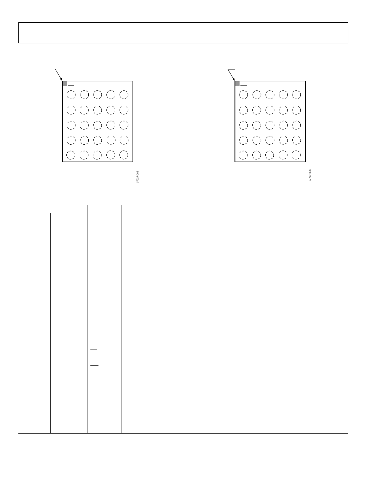
PIN CONFIGURATIONS AND FUNCTION DESCRIPTIONS
BALL A1
INDICATOR
1
2
3
4
5
INT GPIO CIN1 CIN3 CIN5
A
CS TP CIN2 CIN6 CIN7
B
SCLK VDRIVE CIN4 CIN8 CIN9
C
SDI VCC CIN0 CIN10 CIN11
D
SDO GND BIAS ACSHIELD CIN12
E
TOP VIEW
(BALL SIDE DOWN)
Not to Scale
NOTES
1. TP DENOTES FACTORY TEST POINT.
Figure 5. AD7147A Pin Configuration
BALL A1
INDICATOR
1
2
3
4
5
INT GPIO CIN1 CIN3 CIN5
A
ADD1 TP CIN2 CIN6 CIN7
B
SCLK VDRIVE CIN4 CIN8 CIN9
C
ADD0 VCC CIN0 CIN10 CIN11
D
SDA GND BIAS ACSHIELD CIN12
E
TOP VIEW
(BALL SIDE DOWN)
NOTES
Not to Scale
1. TP DENOTES FACTORY TEST POINT.
Figure 6. AD7147A-1 Pin Configuration
Table 7. Pin Function Descriptions
Pin No.
AD7147A AD7147A-1 Mnemonic
B4
B4
CIN6
B5
B5
CIN7
C4
C4
CIN8
C5
C5
CIN9
D4
D4
CIN10
D5
D5
CIN11
E5
E5
CIN12
E4
E4
ACSHIELD
E3
E3
BIAS
E2
E2
GND
D2
D2
C2
C2
E1
N/A
VCC
VDRIVE
SDO
N/A
E1
SDA
D1
N/A
SDI
N/A
D1
ADD0
C1
C1
SCLK
B1
N/A
CS
N/A
B1
ADD1
A1
A1
INT
A2
A2
GPIO
D3
D3
CIN0
A3
A3
CIN1
B3
B3
CIN2
A4
A4
CIN3
C3
C3
CIN4
A5
A5
CIN5
B2
B2
Description
Capacitance Sensor Input.
Capacitance Sensor Input.
Capacitance Sensor Input.
Capacitance Sensor Input.
Capacitance Sensor Input.
Capacitance Sensor Input.
Capacitance Sensor Input.
CDC Active Shield Output. Connect to external shield or plane.
Bias Node for Internal Circuitry. Requires 100 nF capacitor to ground.
Ground Reference Point for All Circuitry.
Supply Voltage.
Serial Interface Operating Voltage Supply.
SPI Serial Data Output.
I2C Serial Data Input/Output. SDA requires pull-up resistor.
SPI Serial Data Input.
I2C Address Bit 0.
Clock Input for Serial Interface.
SPI Chip Select Signal.
I2C Address Bit 1.
General-Purpose Open-Drain Interrupt Output. Programmable polarity; requires pull-up resistor.
Programmable General-Purpose Input/Output.
Capacitance Sensor Input.
Capacitance Sensor Input.
Capacitance Sensor Input.
Capacitance Sensor Input.
Capacitance Sensor Input.
Capacitance Sensor Input.
Factory Test Point Only. Tie to ground.
Rev. B | Page 8 of 68
Share Link: 