2N3904G-AB3-B 查看數據表(PDF) - Unisonic Technologies
零件编号
产品描述 (功能)
生产厂家
2N3904G-AB3-B Datasheet PDF : 4 Pages
| |||
2N3904
NPN SILICON TRANSISTOR
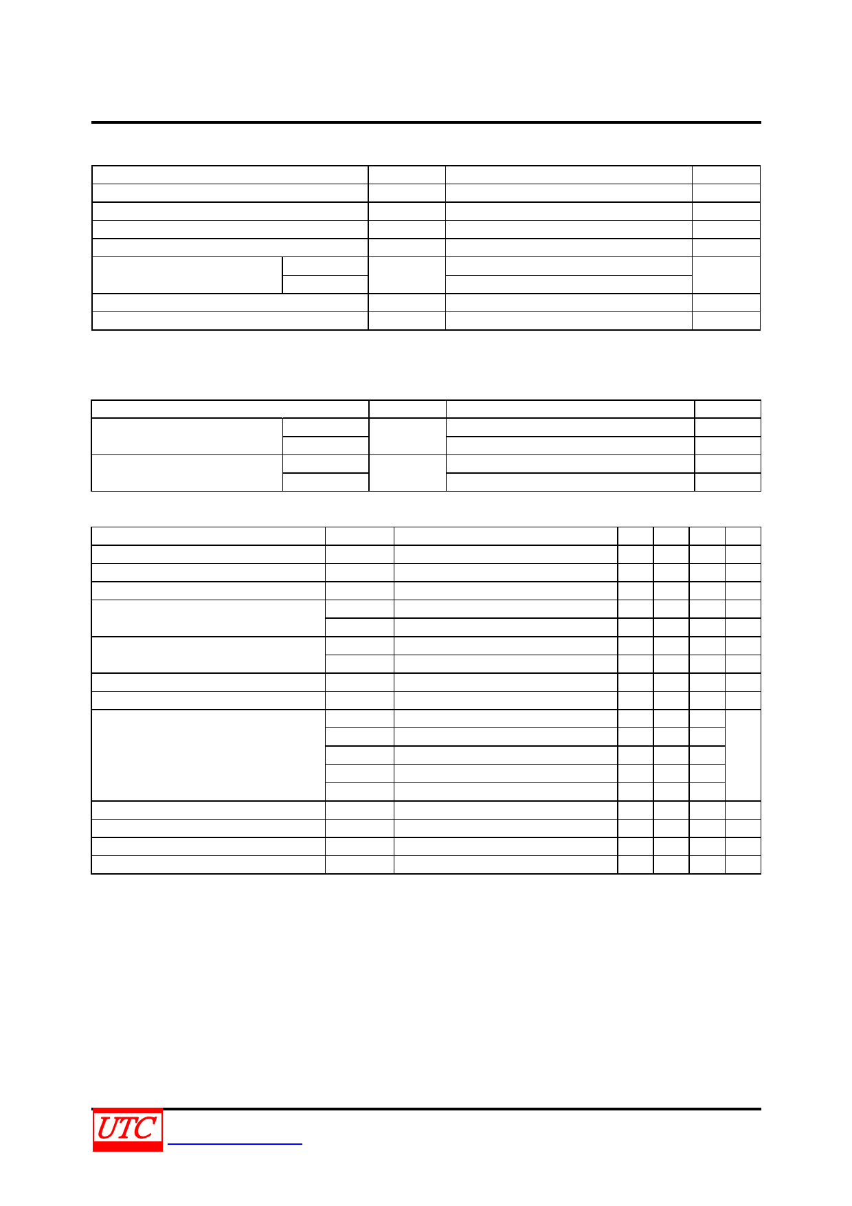
ABSOLUTE MAXIMUM RATING (TA=25°С, unless otherwise specified)
PARAMETER
SYMBOL
RATINGS
UNIT
Collector-Base Voltage
VCBO
60
V
Collector-Emitter Voltage
Emitter-Base Voltage
VCEO
40
V
VEBO
6
V
Collector Current
Collector Dissipation
IC
SOT-89
TO-92
PC
200
mA
500
625
mW
Junction Temperature
TJ
+150
°С
Operating and Storage Temperature
TSTG
-55 ~ +150
°С
Note: Absolute maximum ratings are those values beyond which the device could be permanently damaged.
Absolute maximum ratings are stress ratings only and functional device operation is not implied.
THERMAL DATA
PARAMETER
Junction to Ambient
Junction to Case
SOT-89
TO-92
SOT-89
TO-92
SYMBOL
θJA
θJC
RATING
220
200
38
83.3
ELECTRICAL CHARACTERISTICS (TA=25°С, unless otherwise specified)
UNIT
°C/W
°C/W
°C/W
°C/W
PARAMETER
SYMBOL
TEST CONDITIONS
Collector-Base Breakdown Voltage
Collector-Emitter Breakdown Voltage
BVCBO IC=10A, IE=0
BVCEO IC=1mA,IB=0 (Note)
Emitter-Base Breakdown Voltage
Collector-Emitter Saturation Voltage
(Note)
Base-Emitter Saturation Voltage
(Note)
Collector Cut-off Current
BVEBO
VCE(SAT)1
VCE(SAT)2
VBE(SAT)1
VBE(SAT)2
ICBO
IE=10A, IC=0
IC=10mA, IB=1mA
IC=50mA, IB=5mA
IC=10mA, IB=1mA
IC=50mA, IB=5mA
VCE=30V, VEB=3V
Base Cut-off Current
IBL
hFE1
VCE=30V, VEB=3V
VCE=1V, IC=0.1mA
DC Current Gain (note)
hFE2
hFE3
VCE=1V, IC=1mA
VCE=1V, IC=10mA
hFE4
hFE5
VCE=1V, IC=50mA
VCE=1V, IC=100mA
Current Gain Bandwidth Product
Output Capacitance
fT
VCE=20V, IC=10mA, f=100MHz
COB VCB=5V, IE=0, f=1MHz
Turn on Time
tON VCC=3V,VBE=0.5V,IC=10mA, IB1=1mA
Turn off Time
tOFF IB1=1B2=1mA
Note: Pulse test: Pulse Width≦300s, Duty Cycle≦2%
MIN TYP MAX UNIT
60
V
40
V
6
V
0.2 V
0.3 V
0.65
0.85 V
0.95 V
50 nA
50 nA
40
70
100
300
60
30
300
MHz
4 pF
70 ns
250 ns
UNISONIC TECHNOLOGIES CO., LTD
www.unisonic.com.tw
2 of 4
QW-R201-027.G
Share Link: 