BR24G04FJ-3A 查看數據表(PDF) - ROHM Semiconductor
零件编号
产品描述 (功能)
生产厂家
BR24G04FJ-3A Datasheet PDF : 36 Pages
| |||
BR24G04-3A
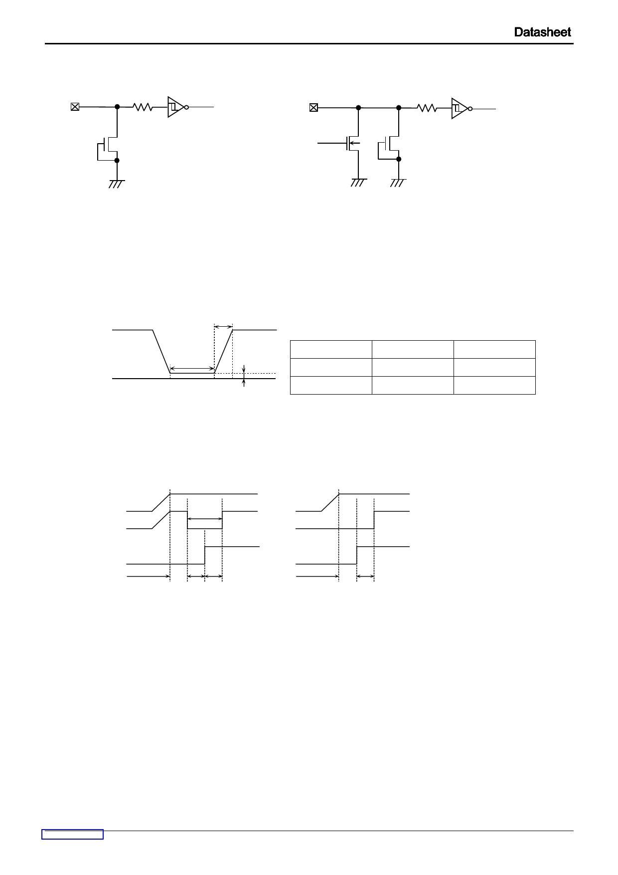
●I/O Equivalence Circuit
○ Input (A2,A1,SCL, WP)
○Input / output (SDA)
Figure 50. Input pin circuit diagram
Figure 51. Input / output pin circuit diagram
●Power-up / Down Conditions
At power on, in IC internal circuit and set, Vcc rises through unstable low voltage area, and IC inside is not completely reset,
and malfunction may occur. To prevent this, functions of POR circuit and LVCC circuit are equipped. To assure the action,
observe the following conditions at power on.
1. Set SDA = 'H' and SCL ='L' or 'H’
2. Start power source so as to satisfy the recommended conditions of tR, tOFF, and Vbot for operating POR circuit.
tR
VCC
Recommended conditions of tR, tOFF,Vbot
tR
tOFF
Vbot
tOFF
Vbot
0
Figure 52. Rise waveform diagram
10ms or below
100ms or below
10ms or larger
10ms or larger
0.3V or below
0.2V or below
3. Set SDA and SCL so as not to become 'Hi-Z'.
When the above conditions 1 and 2 cannot be observed, take the following countermeasures.
a) In the case when the above condition 1 cannot be observed. When SDA becomes 'L' at power on .
→Control SCL and SDA as shown below, to make SCL and SDA, 'H' and 'H'.
VCC
SCL
tLOW
SDA
After Vcc becomes stable
tDH tSU:DAT
Figure 53. When SCL= 'H' and SDA= 'L'
After Vcc becomes stable
tSU:DAT
Figure 54. When SCL='L' and SDA='L'
b) In the case when the above condition 2 cannot be observed.
→After power source becomes stable, execute software reset(P18).
c) In the case when the above conditions 1 and 2 cannot be observed.
→Carry out a), and then carry out b).
●Low Voltage Malfunction Prevention Function
LVCC circuit prevents data rewrite action at low power, and prevents wrong write. At LVCC voltage (Typ. =1.2V) or below, it
prevent data rewrite.
●Noise Countermeasures
○Bypass capacitor
When noise or surge gets in the power source line, malfunction may occur, therefore, for removing these, it is recommended
to attach a by pass capacitor (0.1μF) between IC Vcc and GND. At that moment, attach it as close to IC as possible.
And, it is also recommended to attach a bypass capacitor between board Vcc and GND.
www.rohm.com
© 2014 ROHM Co., Ltd. All rights reserved.
TSZ22111 • 15 • 001
22/33
TSZ02201-0R2R0G100560-1-2
11.Jun.2019 Rev.004
Share Link: 