UAA3535 View Datasheet(PDF) - Philips Electronics
Part Name
Description
Manufacturer
UAA3535 Datasheet PDF : 24 Pages
| |||
Philips Semiconductors
Low power GSM/DCS/PCS multi-band transceiver
Objective specification
UAA3535HL
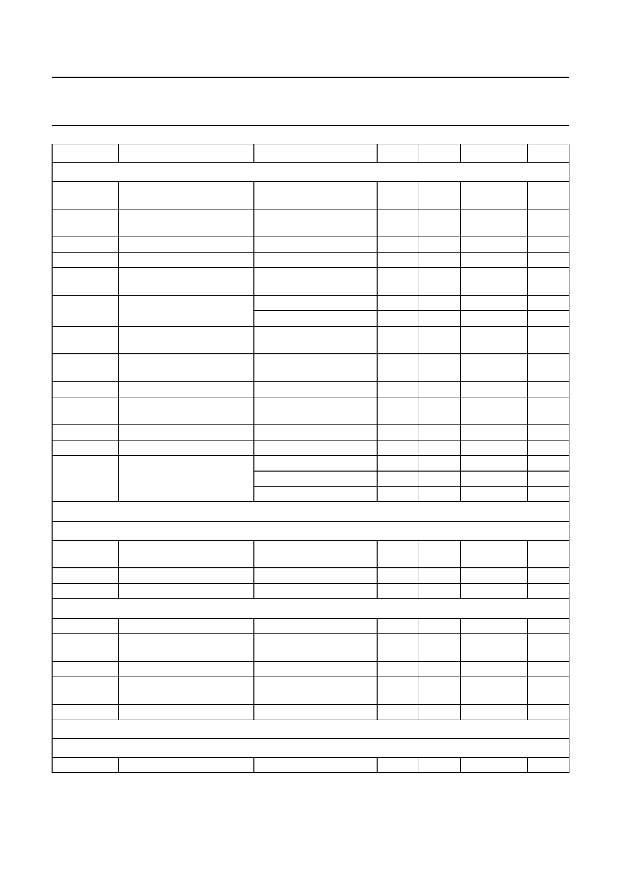
SYMBOL
PARAMETER
CONDITIONS
MIN. TYP.
MAX.
UNIT
PINS IA, IB, QA AND QB (RX MODE)
Gv(min)
minimum voltage conversion gain set to minimum;
19
25
31
dB
gain
notes 1 and 5
Gv(max)
maximum voltage conversion gain set to maximum;
89
93
97
dB
gain
notes 1 and 5
Gv(step)
∆Gv(I/Q)
∆Φ
voltage conversion gain step
gain mismatch I and Q paths
quadrature-phase error
I and Q paths
note 5
note 5
peak error
−
4
−
dB
−
−
0.5
dB
−
−
5
deg
LEAGC
gain control linearity
over full gain range; note 2 −2
−
+2
dB
over any 20 dB gain range −0.5 −
+0.5
dB
Vo(peak)
maximum output voltage per 3% T.H.D.; RL = 100 kΩ 0.75 −
−
V
pin
per pin
Io(peak)
maximum output current per
pin
25
50
−
µA
Voffset
output offset voltage
under static conditions
−300 −
+300
mV
HP−3dB
−3 dB high-pass corner
frequency
4
6
8
kHz
BIF(−3dB)
−3 dB IF filter bandwidth
100 kHz centre frequency 220
−
250
kHz
∆td(g)
group delay variation
30 kHz < fo < 170 kHz
−
1.5
2
µs
α5(IF)
IF filter attenuation
fo = 100 kHz ± 200 kHz 17
31
−
dB
(fifth-order)
fo = 100 kHz ± 400 kHz 54
64
−
dB
fo = 100 kHz ± 600 kHz 73
82
−
dB
Transmit IF section (initial conditions: Vmod(peak) = 0.5 V; fmod = 67.7 kHz; unless otherwise specified)
PINS IA, IB, QA AND QB (TX MODE)
fmod
modulation frequency
3 dB low-pass cut-off
1
−
frequency
Vmod(peak)
modulation level
single-ended; peak value −
0.5
Ri(D)
dynamic input resistance
single-ended
−
25
IF LO oscillator (measured and guaranteed on demonstration board at Tamb = 25 °C)
fIFLO
KVCO
Vtune
∆fVCC
range of possible operation with programming
78
−
VCO gain
Vtune from 0.6 V to
VCC − 0.6 V
−
30
tuning voltage
referenced to VCC(IFCP)
0.4
−
frequency variation with
pushing
respect to the supply voltage
−
−
∆fTRON
frequency variation
pulling
−5
−
Transmit modulation loop section
−
0.55
−
91
−
VCC − 0.4
1
+5
MHz
V
kΩ
MHz
MHz/V
V
MHz/V
kHz
OFFSET MIXER; PIN TXRFI
fRF
RF input frequency
880
−
1 910
MHz
2000 Feb 17
14
Share Link: 