TDA8932T View Datasheet(PDF) - NXP Semiconductors.
Part Name
Description
Manufacturer
TDA8932T Datasheet PDF : 45 Pages
| |||
NXP Semiconductors
TDA8932
Class-D audio amplifier
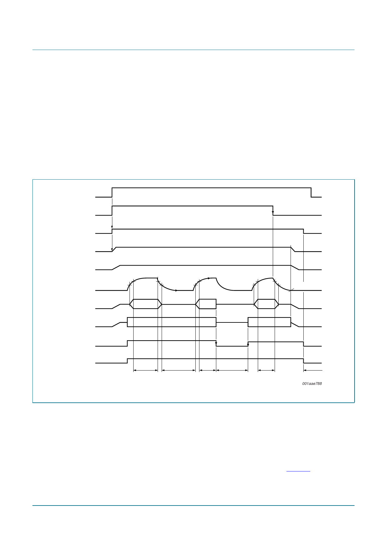
If the transition between Mute mode and Operating mode is controlled via a time constant,
the start-up will be pop free since the DC output offset voltage is applied gradually to the
output between Mute mode and Operating mode. The bias current setting of the
VI-converters is related to the voltage on pin ENGAGE:
• Mute mode: the bias current setting of the VI-converters is zero (VI-converters
disabled)
• Operating mode: the bias current is at maximum
The time constant required to apply the DC output offset voltage gradually between Mute
mode and Operating mode can be generated by applying a decoupling capacitor on pin
ENGAGE. The value of the capacitor on pin ENGAGE should be 470 nF.
VP
POWERUP
DREF
HVPREF
HVP1, HVP2
0.43VENGAGE
ENGAGE 0.3VENGAGE
audio
OUT1, OUT2
PWM
AUDIO
PWM
AUDIO
AUDIO
PWM
0.17VENGAGE
DIAG
OSCIO
Fig 3. Start-up sequence
operating
mute
operating fault
operating
sleep
001aae788
8.3 Pulse width modulation frequency
The output signal of the amplifier is a PWM signal with a carrier frequency of
approximately 320 kHz. Using a 2nd-order low-pass filter in the application results in an
analog audio signal across the loudspeaker. The PWM switching frequency can be set by
an external resistor Rosc connected between pins OSCREF and VSSD(HW). The carrier
frequency can be set between 300 kHz and 500 kHz. Using an external resistor of 39 kΩ,
the carrier frequency is set to an optimized value of 320 kHz (see Figure 4).
TDA8932_2
Preliminary data sheet
Rev. 02 — 12 December 2006
© NXP B.V. 2006. All rights reserved.
7 of 45
Share Link: 