25VF080 View Datasheet(PDF) - Silicon Storage Technology
Part Name
Description
Manufacturer
25VF080 Datasheet PDF : 23 Pages
| |||
8 Mbit SPI Serial Flash
SST25VF080
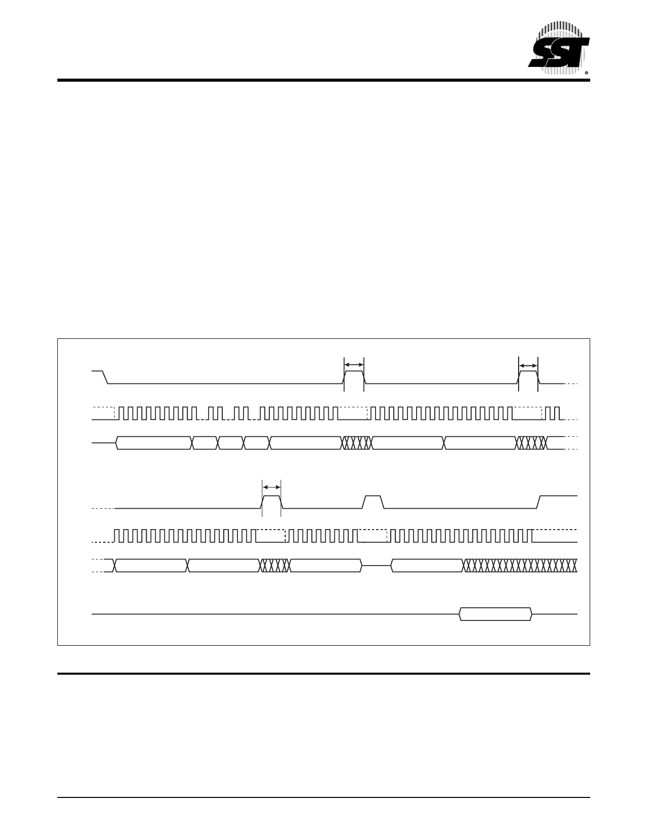
Auto Address Increment (AAI) Program
The AAI program instruction allows multiple bytes of data to
be programmed without re-issuing the next sequential
address location. This feature decreases total program-
ming time when the entire memory array is to be pro-
grammed. An AAI program instruction pointing to a
protected memory area will be ignored. The selected
address range must be in the erased state (FFH) when ini-
tiating an AAI program instruction.
Prior to any write operation, the Write-Enable (WREN)
instruction must be executed. The AAI program instruction
is initiated by executing an 8-bit command, AFH, followed
by address bits [A23-A0]. Following the addresses, the data
is input sequentially from MSB (Bit 7) to LSB (Bit 0). CE#
must be driven high before the AAI program instruction is
executed. The user must poll the BUSY bit in the software
Advance Information
status register or wait TBP for the completion of each inter-
nal self-timed Byte-Program cycle. Once the device com-
pletes programming byte, the next sequential address may
be program, enter the 8-bit command, AFH, followed by the
data to be programmed. When the last desired byte had
been programmed, execute the Write-Disable (WRDI)
instruction, 04H, to terminate AAI. After execution of the
WRDI command, the user must poll the Status register to
ensure the device completes programming. See Figure 6
for AAI programming sequence.
There is no wrap mode during AAI programming; once the
highest unprotected memory address is reached, the
device will exit AAI operation and reset the Write-Enable-
Latch bit (WEL = 0).
TBP
TBP
CE#
MODE 3 0 1 2 3 4 5 6 7 8 15 16 23 24 31 32 33 34 35 36 37 38 39
0 1 2 3 4 5 6 7 8 9 10 11 12 13 14 15
01
SCK MODE 0
SI
AF
A[23:16] A[15:8] A[7:0]
Data Byte 1
AF
Data Byte 2
TBP
CE#
SCK
0 1 2 3 4 5 6 7 8 9 10 11 12 13 14 15
01234567
0 1 2 3 4 5 6 7 8 9 10 11 12 13 14 15
SI
AF
Last Data Byte
04
05
Write Disable (WRDI)
Read Status Register (RDSR)
Instruction to terminate Instruction to verify end of
AAI Operation
AAI Operation
SO
DOUT
FIGURE 6: AUTO ADDRESS INCREMENT (AAI) PROGRAM SEQUENCE
1250 F06.0
©2003 Silicon Storage Technology, Inc.
11
S71250-00-000
10/03
Share Link: 