LA76070 View Datasheet(PDF) - SANYO -> Panasonic
Part Name
Description
Manufacturer
LA76070 Datasheet PDF : 27 Pages
| |||
LA76070
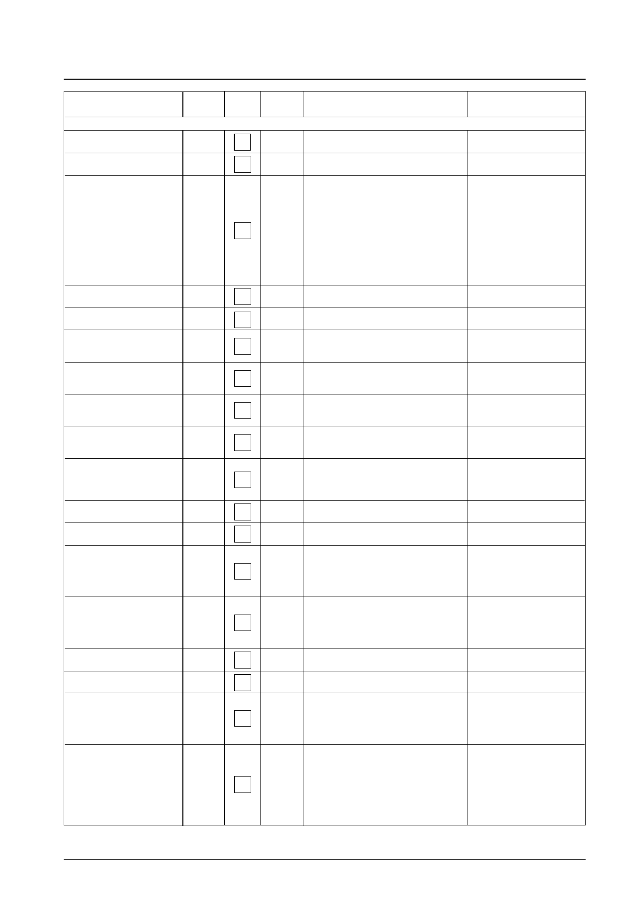
Parameter
Symbol
Measurement
point
Input signal
Measurement procedure
Bus conditions
[VIF Block]
AFT output voltage with no signal VAFTn
13
Video output voltage with no signal
VOn
45
APC pull-in range (U), (L)
fPU, fPL 45
Maximum RF AGC voltage
Minimum RF AGC voltage
RF AGC Delay Pt
(@DAC = 0)
RF AGC Delay Pt
(@DAC = 63)
VRFH
6
VRFL
6
RFAGC0
6
6 RFAGC63
Maximum AFT output voltage
VAFTH 13
Minimum AFT output voltage
VAFTL 13
AFT detection sensitivity
VAFTS 13
Video output amplitude
Synchronization signal tip level
VO
45
VOtip
45
Input sensitivity
Vi
45
Video-to-sync ratio (@ 100 dBµ)
V/S
45
Differential gain
Differential phase
Video signal-to-noise ratio
DG
45
DP
45
S/N
45
920 kHz beat level
I920
45
Measure the pin 13 DC voltage when
No signal IF.AGC. DEF is "1"
After performing the adjustments
described in section 4
Measure the pin 45 DC voltage when
No signal IF.AGC. DEF is "1"
After performing the adjustments
described in section 4
SG4
93 dBµ
Connect an oscilloscope to pin 45 and modify
the SG4 signal to be a frequency above 45.75
MHz so that the PLL circuit becomes unlocked.
(Beating will occur in this state.) Gradually
lower the SG4 frequency and measure the
frequency at which the PLL circuit locks.
Similarly, modify the frequency to a value
below 45.75 MHz so that the PLL circuit
becomes unlocked. Gradually raise the SG4
frequency and measure the frequency at which
the PLL circuit locks.
After performing the adjustments
described in section 4
SG1 Set the RF AGC DAC to 0 and measure the pin After performing the adjustments
91 dBµ 6 DC voltage
described in section 4
SG1 Set the RF AGC DAC to 63 and measure the
91 dBµ pin 6 DC voltage
After performing the adjustments
described in section 4
SG1
Set the RF AGC DAC to 0 and determine the
input level such that the pin 6 DC voltage
becomes 3.8 V ±0.5 V
After performing the adjustments
described in section 4
SG1
Set the RF AGC DAC to 63 and determine the
input level such that the pin 4 DC voltage
becomes 3.8 V ±0.5 V
After performing the adjustments
described in section 4
SG4
93 dBµ
Set the SG4 signal frequency to 44.75 MHz
and input that signal. Measure the pin 13 DC
voltage at that time.
After performing the adjustments
described in section 4
SG4
93 dBµz
Set the SG4 signal frequency to 46.75 MHz
and input that signal. Measure the pin 13 DC
voltage at that time.
After performing the adjustments
described in section 4
SG4
93 dBµz
Modify the SG4 frequency to determine the
frequency deviation (∆f) such that the pin
13 DC voltage changes from 2.5 V to 5.0 V.
VAFTS = 2500/∆f [mV/kHz]
After performing the adjustments
described in section 4
SG7 Observe pin 45 with an oscilloscope and
93 dBµ measure the p-p value of the waveform
After performing the adjustments
described in section 4
SG1
93 dBµ Measure the pin 45 DC voltage
After performing the adjustments
described in section 4
SG7
Observe pin 45 with an oscilloscope and measure
the peak-to-peak value of the waveform. Next,
gradually lower the input level to determine the input
level such that the output becomes –3 dB below the
video signal amplitude VO.
After performing the adjustments
described in section 4
SG7
100 dBµ
Observe pin 45 with an oscilloscope and
determine the value of the Vy/Vs ratio by
measuring the peak-to-peak value of the sync
After performing the adjustments
described in section 4
waveform (Vs) and the peak-to-peak value of the
luminance signal (Vy).
SG5
93 dBµ Measure pin 45 with a vectorscope
After performing the adjustments
described in section 4
SG5
93 dBµ Measure pin 45 with a vectorscope
After performing the adjustments
described in section 4
SG1
93 dBµ
Pass the noise voltage that occurs on pin
45 through a 10 kHz to 4 MHz bandpass filter,
measure that voltage (Vsn) with an rms
voltmeter. Use that value to calculate 20 × log
(1.43/Vsn).
After performing the adjustments
described in section 4
SG1
SG2
SG3
Input SG1 at 93 dBµ and measure the pin
12 DC voltage (V12).Mix three signals: SG1 at
87 dBµ, SG2 at 82 dBµ, and SG3 at 63 dBµ,
and input that signal to VIF IN. Now, apply the
V12 voltage to pin 12 using an external power
supply. Measure the difference between the
3.58 MHz component and the 920 kHz
component with a spectrum analyzer.
After performing the adjustments
described in section 4
No. 5844-11/27
Share Link: 