LC8390M View Datasheet(PDF) - SANYO -> Panasonic
Part Name
Description
Manufacturer
LC8390M Datasheet PDF : 12 Pages
| |||
LC8390M
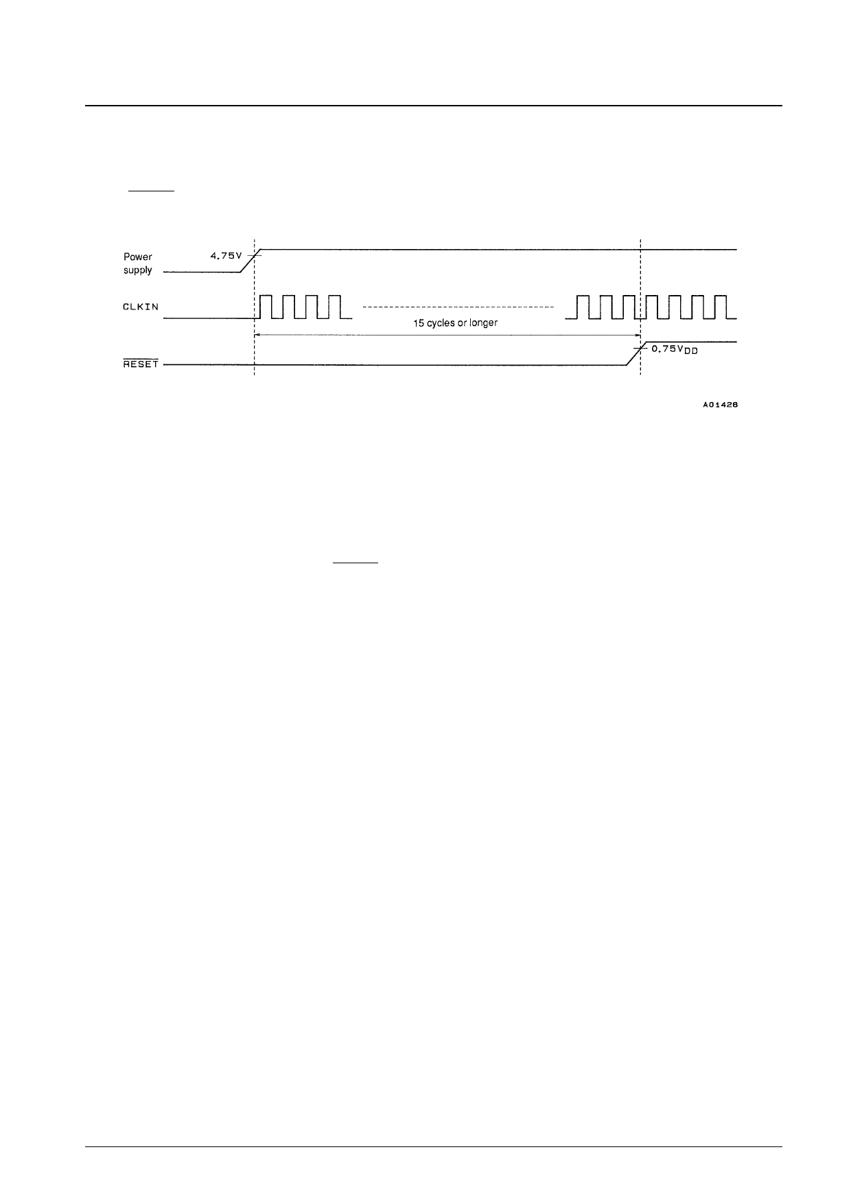
3. Initialization
The LC8390M must be initialized after power is applied and when the sampling period changes. To initialize the
LC8390M, once the power supply voltage has stabilized and CLKIN has been supplied, a low level must be input to
the RESET pin for a period longer than 15 CLKIN cycles.
Design and Usage Notes
1. External Clock
The CLKIN must not be stopped during operation. If this clock is not supplied, overcurrents may occur since
dynamic logic is used internally, and the LC8390M may function abnormally. This IC must synchronize its internal
operating timing with the externally supplied ADLRCK and DALRCK. This synchronization is performed by
resetting an internal counter. This reset is only performed a few times on the rising edges of ADLRCK and
DALRCK following initialization by a RESET pin input. Therefore, the CLKIN, ADLRCK, ADBCK, DALRCK and
DABCK clock inputs must be synchronized. However, CLKIN and other clocks do not have to be synchronized for
arbitrary timing input and output. Clock jitter will degrade A/D and D/A converter precision in this IC. The wiring
lines for the master clock must be kept as short as possible, and a crystal oscillator signal level clock should be used.
2. Power Supply and Ground
Use care in supplying power and ground to this IC. Separate the analog and digital blocks, and provide a separate
ground plane for each. Connect the analog and digital grounds to points near the power supply on the PC board.
While DVDD is the power supply for the internal logic circuits, since DVDD and the analog system VDD supplies
(ADLVDD, ADRVDD, DALVDD and DARVDD) are connected together through the IC substrate with a few Ohms
resistance, they should have identical voltages, and care should be exercised in handling the digital system power
supply.
3. A/D Block DC Offset Adjustment
A DC offset component appears in the A/D block digital output due to manufacturing variations in the IC itself and
in resistor values. When there is a DC offset, differences in the full scale level of the analog input are created. It is
therefore necessary to adjust the DC offset adjustment point in the application circuit example (see the section
“LC8390M Application Circuit Example”) while monitoring the digital output, and to cut the DC component by
performing HPF processing in the input processing block of the later stage DSP.
No. 4454-10/12
Share Link: 