LC8390M View Datasheet(PDF) - SANYO -> Panasonic
Part Name
Description
Manufacturer
LC8390M Datasheet PDF : 12 Pages
| |||
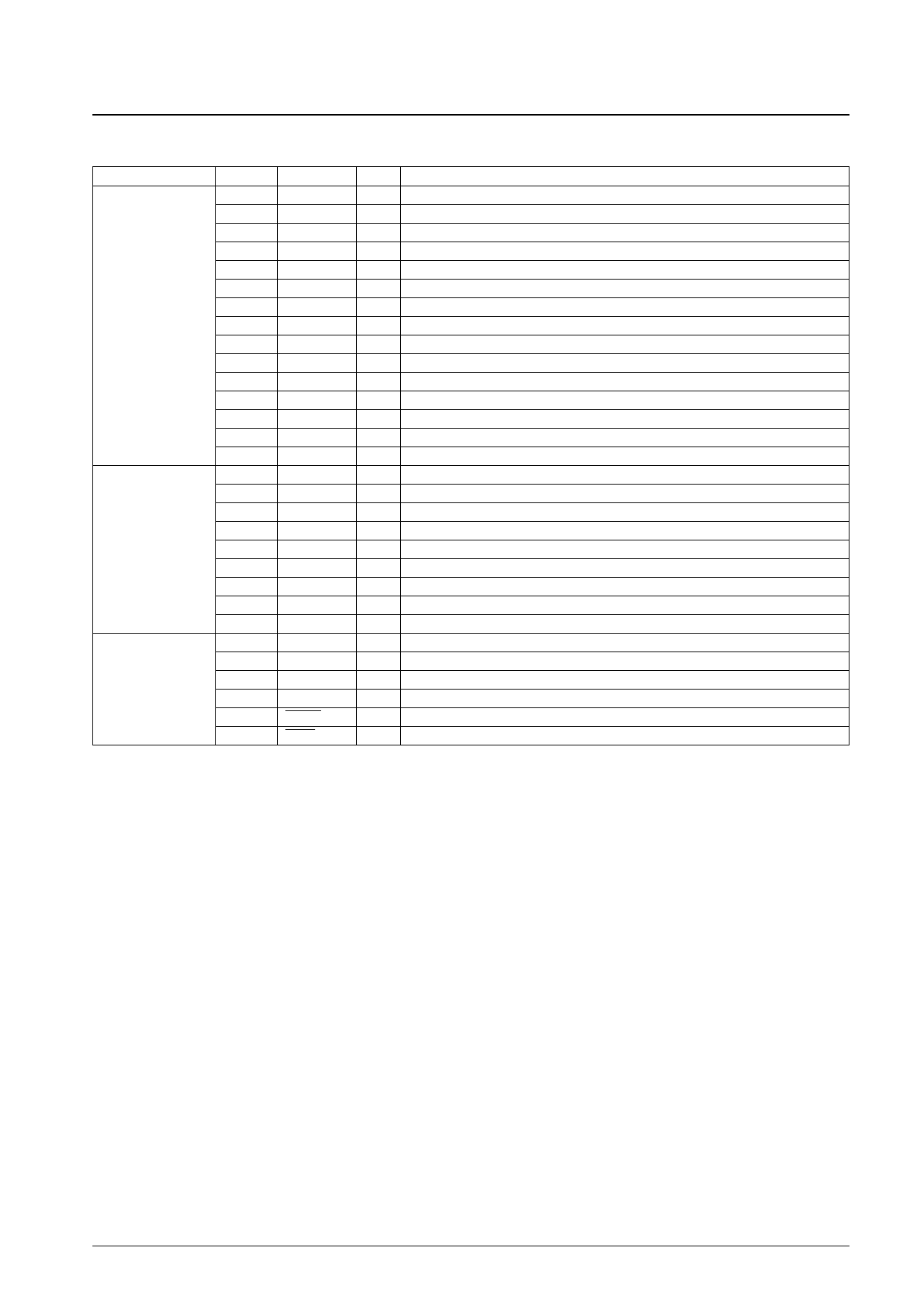
Pin Functions
Block
A/D block
D/A block
Control and other pins
Pin No.
5
3
4
2
6
11
9
10
8
12
26
25
24
1
7
15
13
14
18
16
17
21
20
22
30
19
23
28
27
29
Pin
ADLVDD
ADLVSS
ADL1
ADL2
ADL3
ADRVDD
ADRVSS
ADR1
ADR2
ADR3
ADLRCK
ADBCK
ADDATA
DZOUTL
DZOUTR
DALVDD
DALVSS
PWML
DARVDD
DARVSS
PWMR
DALRCK
DABCK
DADATA
DVDD
DVSS
CLKIN
CLKCTL
RESET
TEST
LC8390M
I/O
Function
— Analog left channel A/D power supply
— Analog left channel A/D ground
I Left channel A/D audio input
O Left channel A/D linear ∆Σ output
O Left channel A/D quadratic ∆Σ output
— Analog right channel A/D power supply
— Analog right channel A/D ground
I Right channel A/D audio input
O Right channel A/D linear ∆Σ output
O Right channel A/D quadratic ∆Σ output
I A/D left and right channel clock input
I A/D bit clock input
O A/D data output
O A/D dithering clock output
O A/D dithering clock output
— Analog left channel D/A power supply
— Analog left channel D/A ground
O Left channel D/A PWM output
— Analog right channel D/A power supply
— Analog right channel D/A ground
O Right channel D/A PWM output
I D/A left and right channel clock input
I D/A bit clock input
I D/A data input
— Digital system power supply
— Digital system ground
I Master clock input
I Master clock selection (high: 512 Fs, low: 384 Fs)
I Reset input
I
Test input. (This pin must be connected to DVDD during normal operation.)
No. 4454-3/12
Share Link: 