SST25VF010 View Datasheet(PDF) - Silicon Storage Technology
Part Name
Description
Manufacturer
SST25VF010 Datasheet PDF : 22 Pages
| |||
1 Mbit SPI Serial Flash
SST25VF010
Chip-Erase
The Chip-Erase instruction clears all bits in the device to
FFH. A Chip-Erase instruction will be ignored if any of the
memory area is protected. Prior to any Write operation, the
Write-Enable (WREN) instruction must be executed. CE#
must remain active low for the duration of the Chip-Erase
instruction sequence. The Chip-Erase instruction is initiated
Data Sheet
by executing an 8-bit command, 60H. CE# must be driven
high before the instruction is executed. The user may poll
the Busy bit in the software status register or wait TCE for
the completion of the internal self-timed Chip-Erase cycle.
See Figure 9 for the Chip-Erase sequence.
CE#
MODE 3
SCK MODE 0
0 1 2345 6 7
SI
60
MSB
SO
HIGH IMPEDANCE
1233 F09.1
FIGURE 9: CHIP-ERASE SEQUENCE
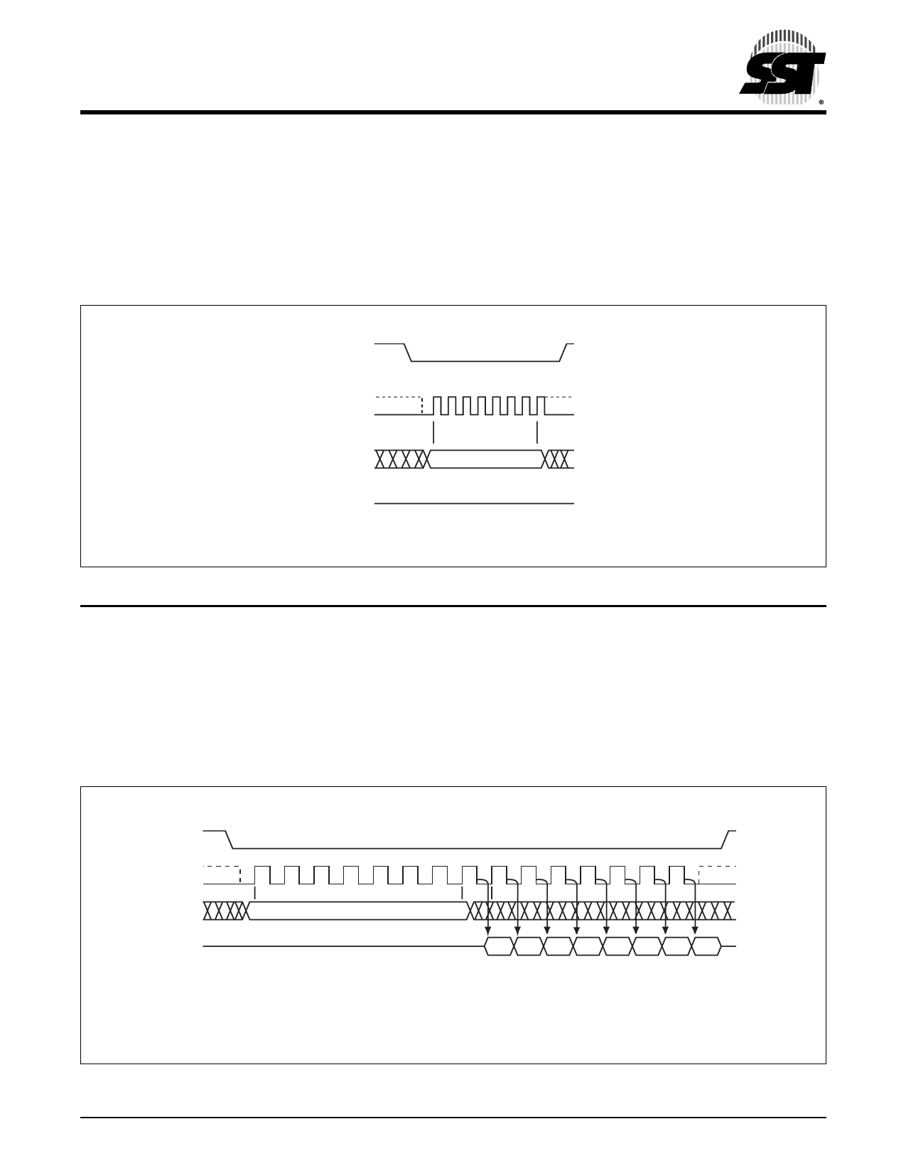
Read-Status-Register (RDSR)
The Read-Status-Register (RDSR) instruction allows read-
ing of the status register. The status register may be read at
any time even during a Write (Program/Erase) operation.
When a Write operation is in progress, the Busy bit may be
checked before sending any new commands to assure that
the new commands are properly received by the device.
CE# must be driven low before the RDSR instruction is
entered and remain low until the status data is read. Read-
Status-Register is continuous with ongoing clock cycles
until it is terminated by a low to high transition of the CE#.
See Figure 10 for the RDSR instruction sequence.
CE#
MODE 3 0
1
2
3
4
5
6
SCK MODE 0
SI
05
MSB
HIGH IMPEDANCE
SO
7
8
9 10 11 12 13 14
Bit 7 Bit 6 Bit 5 Bit 4 Bit 3 Bit 2 Bit 1 Bit 0
MSB
Status
Register Out
1233 F10.1
FIGURE 10: READ-STATUS-REGISTER (RDSR) SEQUENCE
©2003 Silicon Storage Technology, Inc.
11
S71233-01-000
8/03
Share Link: 