F81865F View Datasheet(PDF) - Feature Integration Technology Inc.
Part Name
Description
Manufacturer
F81865F Datasheet PDF : 128 Pages
| |||
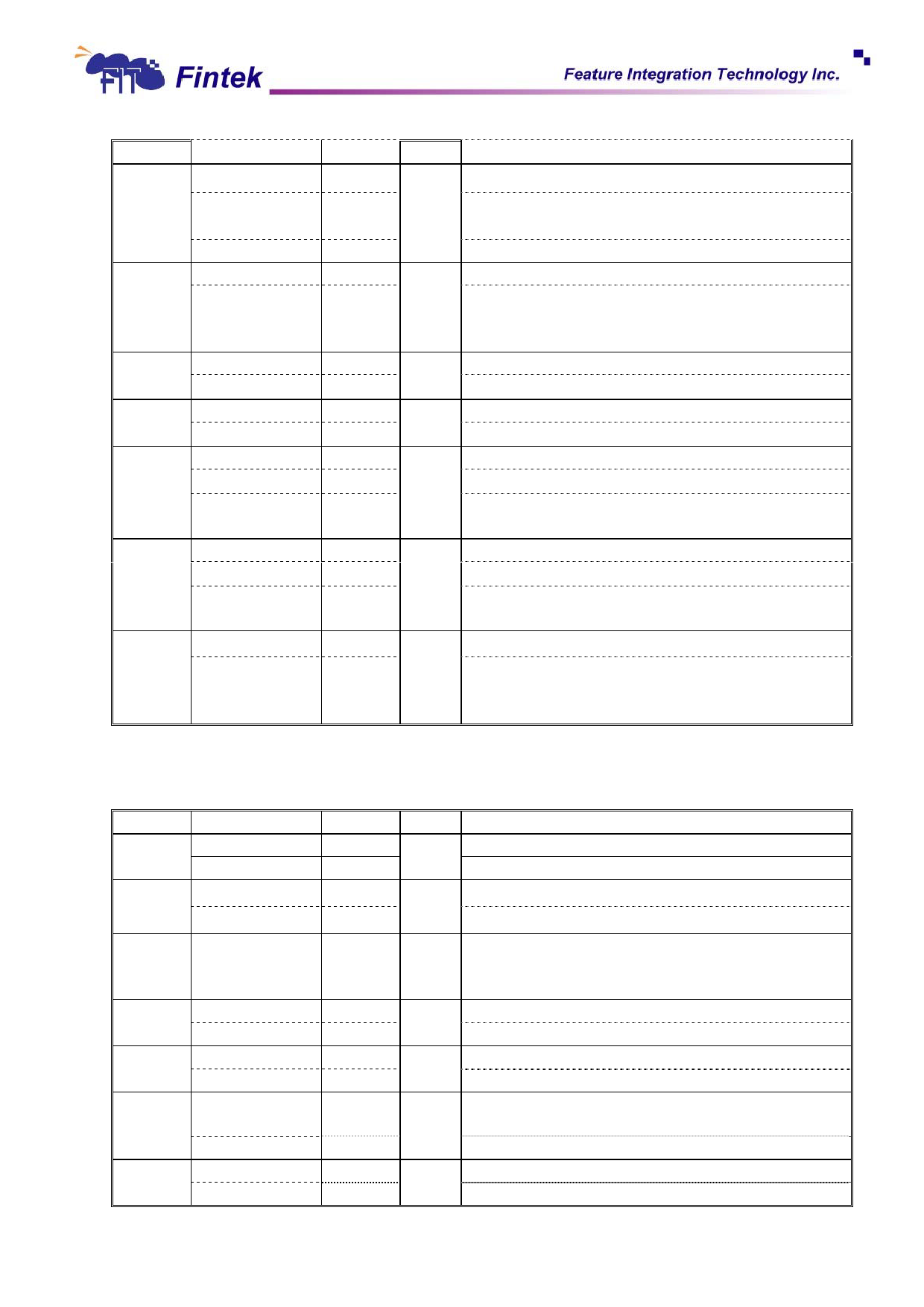
F81865
IRTX_1
GPIO06
O12
I/OOD12t
Infrared Transmitter Output.
General purpose IO.
58
SIN6_1
INt,5v
VSB UART Serial Input. Used to receive serial data
through the communication link.
IRRX_1
INt,5v
Infrared Receiver input.
GPIO07
I/OOD12t
General purpose IO.
59
VSB UART Request To Send. An active low signal informs
RTS6_1#
O12
the modem or data set that the controller is ready to
send data.
65
GPIO10
I/OOD12t VSB General purpose IO.
LED_VSB
OD12
Power LED for VSB.
66
GPIO11
I/OOD12t VSB General purpose IO.
LED_VCC
OD12
Power LED for VCC.
GPIO12
I/OOD12t
General purpose IO.
67
SCL
I/OOD12t VSB SMBus Clock.
UART Serial Output. Used to transmit serial data out
SOUT5
O12
to the communication link.
GPIO13
I/OOD12t
General purpose IO.
68
SDA
I/OOD12t VSB SMBus Data.
UART Serial Output. Used to transmit serial data out
SIN5
INt,5v
to the communication link.
GPIO14
I/OOD12t
General purpose IO.
69
VSB UART Request To Send. An active low signal informs
RTS5#
O12
the modem or data set that the controller is ready to
send data.
6.8 ACPI Function Pins
Pin No.
70
76
Pin Name
WDTRST#
GPIO15
ALERT#
GPIO20
74
PME#
ATXPG_IN
77
GPIO21
PWSIN#
78
GPIO22
PWSOUT#
79
GPIO23
S3#
80
GPIO24
Type
OD12,5v
I/OOD12t
OD12
I/OOD12t
PWR
VSB
VSB
OD12,5v VSB
INst,5v
I/OOD12t
INst,5v
I/OOD12t
OD12
I/OOD12t
INst,5v
I/OOD12t
VSB
VSB
VSB
VSB
Description
Watch dog timer signal output.
General purpose IO.
Alert a signal when temperature over limit setting.
General purpose IO.
Generated PME event. It supports the PCI PME#
interface. This signal allows the peripheral to request
the system to wake up.
ATX Power Good input.
General purpose IO.
Main power switch button input.
General purpose IO.
Panel Switch Output. This pin is low active and pulse
output. It is power on request output#.
General purpose IO.
S3# Input is Main power on-off switch input.
General purpose IO.
18
May, 2010
V0.28P
Share Link: 