IT8673F View Datasheet(PDF) - ITE Tech. INC.
Part Name
Description
Manufacturer
IT8673F Datasheet PDF : 128 Pages
| |||
IT8673F
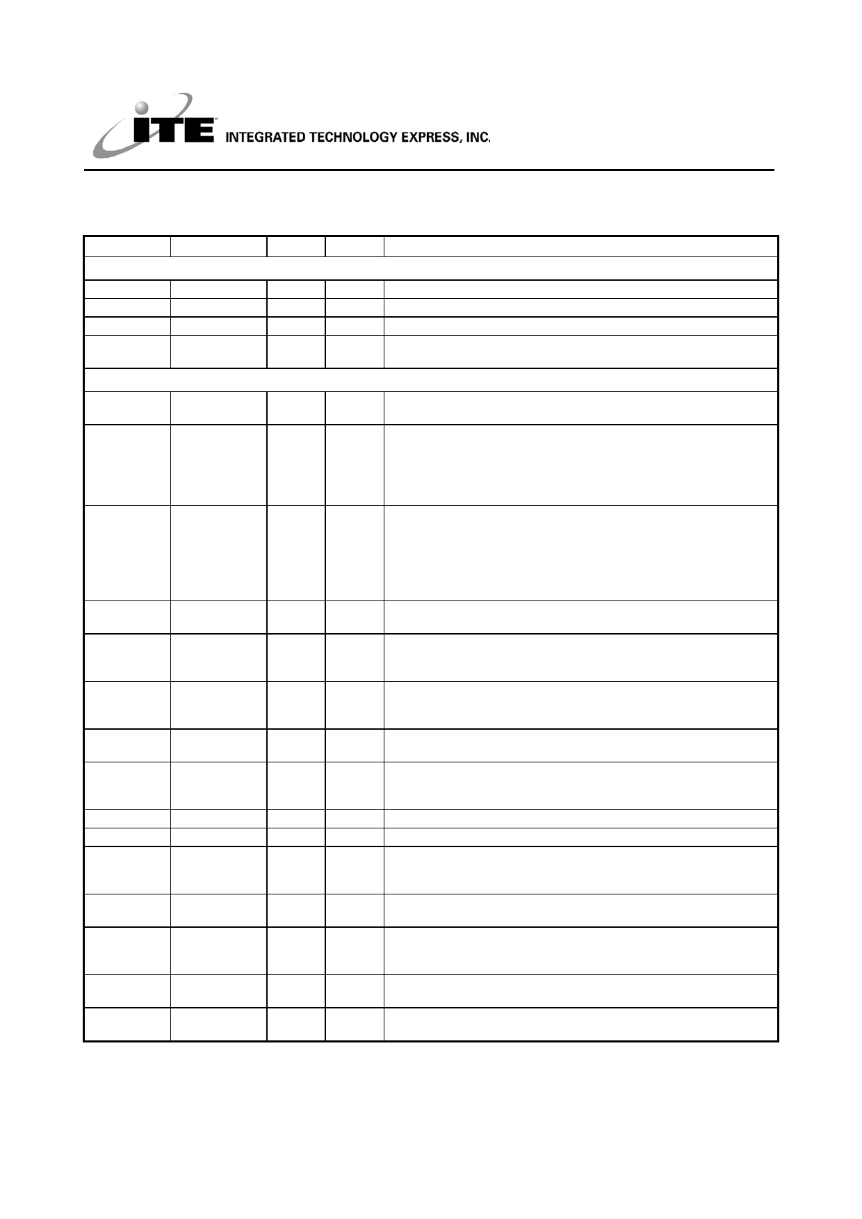
6. IT8673F Pin Descriptions
Table 6-1. Signal Names (by pin numbers in alphabetical order)
Pin(s) No.
Signal
I/O
Supplies
35, 67, 121 VCC
PWR
99
VCCH
PWR
97
VBAT
PWR
4,10,43, 77, GNDD
104
GND
ISA Bus Interface Signals
21-32
SA[0:11]
DI
96
SA15/
DI/
FAN_CTL3
DOD8
95
SA14/
DI/DI
FAN_TAC3
92-91
39 - 42,
44 - 47
118
74 - 76
87 – 89
36
34
119
37
120
38
33
SA[13:12]
SD[0:7]
DI
DIO24
AEN
DI
DRQ[1:3]
DACK[1:3]#
DO8
DI
PCICLK
SIRQ
RESET
DI
DIO24
DI
IOR#
DI
TC
DI
IOW#
IOCHRDY
DI
DOD24
Power
-
-
-
-
VCC
VCCH
VCCH
VCCH
VCC
VCC
VCC
VCCH
VCC
VCC
VCC
VCC
VCC
VCC
VCC
Description
+5V Digital Power Supply.
+5V VCC Help Supply.
+3.3V Battery Supply.
Digital Ground.
ISA Address 0 - 11. Input signals used to determine which internal
register is accessed. SA0-SA11 are ignored during a DMA access.
ISA Address 15 / FAN Control Output 3.
• The default function of this pin is ISA address 15.
• The second function of this pin is the FAN Control Output 3.
• The function of this pin is decided by the power-on strapping of
DTR1#.
ISA Address 14 / FAN Tachometer Input 3.
• The default function of this pin is ISA address 14.
• The second function of this pin is the FAN Tachometer Input 3. (0
to +5V amplitude FAN tachometer input).
• The function of this pin is decided by the power-on strapping of
RTS1#.
ISA Address 13 - 12. Input signals used to determine which internal
register is accessed. SA13-SA12 are ignored during a DMA access.
ISA Data 0 - 7. 8-bit bi-directional data lines used to transfer data
between IT8673F and the CPU or DMA controller. SD0 is the LSB
and SD7 is the MSB.
Address Enable. AEN is used to disable the internal address
decoder when it is high. This pin is always ignored during DMA
accesses.
DMA Request 1 - 3. Active high outputs to signal the DMA controller
that a data transfer from IT8673F is required.
DMA Acknowledge 1 - 3 #. Active low inputs to acknowledge the
corresponding DMA requests and enable the RD or WR signals
during a DMA access cycle.
PCI Clock. the PCI CLOCK input.
Serial Interrupt.
Reset. A high level on this input resets IT8673F. This signal
asynchronously terminates any activity and places the device in the
Disable state.
I/O Read #. Active low input asserted by the CPU or DMA controller
to read data or status information from IT8673F.
Terminal Count. This input is asserted by the DMA controller to
indicate the end of a DMA transfer. The signal is only effective during
a DMA access cycle.
I/O Write #. Active low input asserted by the CPU or DMA controller
to write data or control information to IT8673F.
I/O Channel Ready. Pulled low to extend the Read/Write command
under the EPP mode.
6
Share Link: 