IT8673F View Datasheet(PDF) - ITE Tech. INC.
Part Name
Description
Manufacturer
IT8673F Datasheet PDF : 128 Pages
| |||
IT8673F
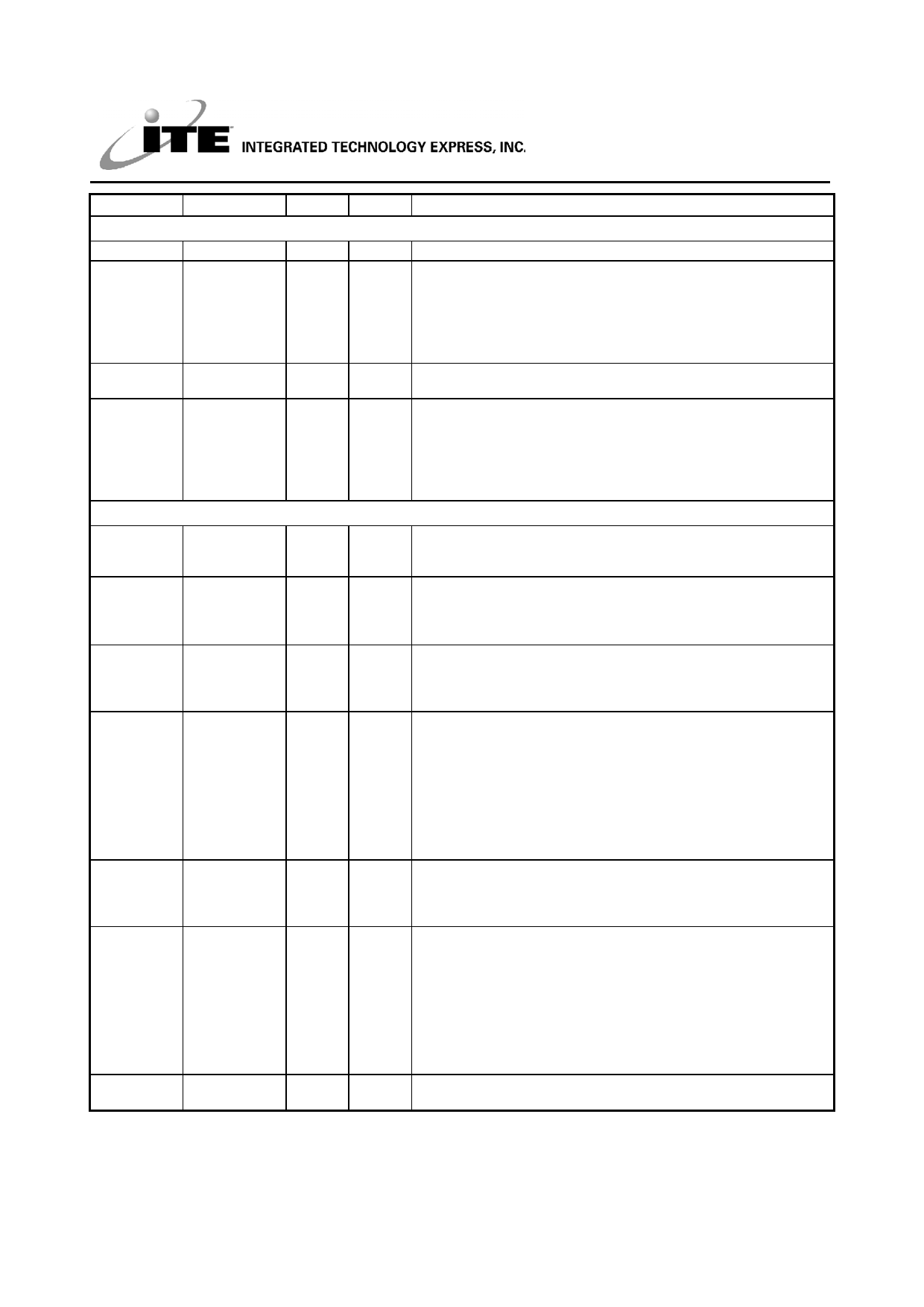
Pin(s) No.
Signal
I/O Power
FAN Speed Controller Signals
65
FAN_CTL1
DOD8 VCC
72
FAN_CTL2/ DOD8/ VCC
GP13
DIOD8
64
FAN_TAC1
DI
VCC
73
FAN_TAC2/
DI/
VCC
GP12
DIOD8
Serial Port 1 Signals
52
CTS1#
DI
VCC
55
DCD1#
DI
VCC
50
DSR1#
DI
VCC
53
DTR1#/
DO8/DI VCC
PIN96SEL
54
RI1#
DI
VCC
51
RTS1#/
DO8/DI VCC
PIN95SEL
48
SIN1
DI
VCC
Description
FAN Control Output 1. (PWM output signal to FAN’s FET.)
FAN Control Output 2 / General Purpose I/O 13.
• The default function of this pin is FAN Control Output 2 (PWM
output signal to FAN’s FET).
• The second function of this pin is the GP13.
• The function configuration of this pin is decided by the GPIO
configuration registers.
FAN Tachometer Input 1. (0 to +5V amplitude FAN tachometer
input)
FAN Tachometer Input 2 / General Purpose I/O 12.
• The default function of this pin is FAN Tachometer Input 2. (0 to
+5V amplitude FAN tachometer input)
• The second function of this pin is the GP12.
• The function configuration of this pin is decided by the GPIO
configuration registers.
Clear to Send 1 #. When low, indicates that the MODEM or Data
Set is ready to accept data. The CTS# signal is a MODEM status
input whose condition can be tested by reading the MSR register.
Data Carrier Detect 1 #. When low, indicates that the MODEM or
Data Set has detected a carrier. The DCD# signal is a MODEM
status input whose condition can be tested by reading the MSR
register.
Data Set Ready 1 #. When low, indicates that the MODEM or Data
Set is ready to establish a communications link. The DSR# signal is
a MODEM status input whose condition can be tested by reading the
MSR register.
Data Terminal Ready 1 # / Pin 96 Multiplex Select .
• The default function of this pin is Data Terminal Ready 1 #. The
DTR# signal is used to indicate to the MODEM or Data Set that the
device is ready to exchange data. DTR# is activated by setting the
appropriate bit in the MCR register to 1. After a Master Reset
operation or during Loop mode, DTR# is set to its inactive state.
• The second function of this pin is the power-on strapping of Pin 96
multiplex select. When high, the pin 96 is selected as SA15. This
pin is weak pull-up internally.
Ring Indicator 1 #. When low, indicates that a telephone ring signal
has been received by the MODEM. The RI# signal is a MODEM
status input whose condition can be tested by reading the MSR
register.
Request to Send 1 # / Pin 95 Multiplex Select.
• The default function of this pin is Request To Send 1 #. When low,
this output indicates to the MODEM or Data Set that the device is
ready to send data. RTS# is activated by setting the appropriate
bit in the MCR register to 1. After a Master Reset operation or
during Loop mode, RTS# is set to its inactive state.
• The second function of this pin is the power-on strapping of Pin 95
multiplex select. When high, the pin 95 is selected as SA14. This
pin is weak pull-up internally.
Serial Data In 1. This input receives serial data from the
communications link.
7
Share Link: 