LT3669 View Datasheet(PDF) - Linear Technology
Part Name
Description
Manufacturer
LT3669 Datasheet PDF : 40 Pages
| |||
LT3669/LT3669-2
APPLICATIONS INFORMATION
and safe operation, the LT3669 will only synchronize
when the output voltage is near regulation. Therefore, it
is necessary to choose a large enough inductor value to
supply the required output current at the frequency set
by the RT resistor. See the Inductor Selection section for
more information. It is also important to note that slope
compensation is set by the RT value. To avoid subhar-
monics, calculate the minimum inductor value using the
frequency determined by RT.
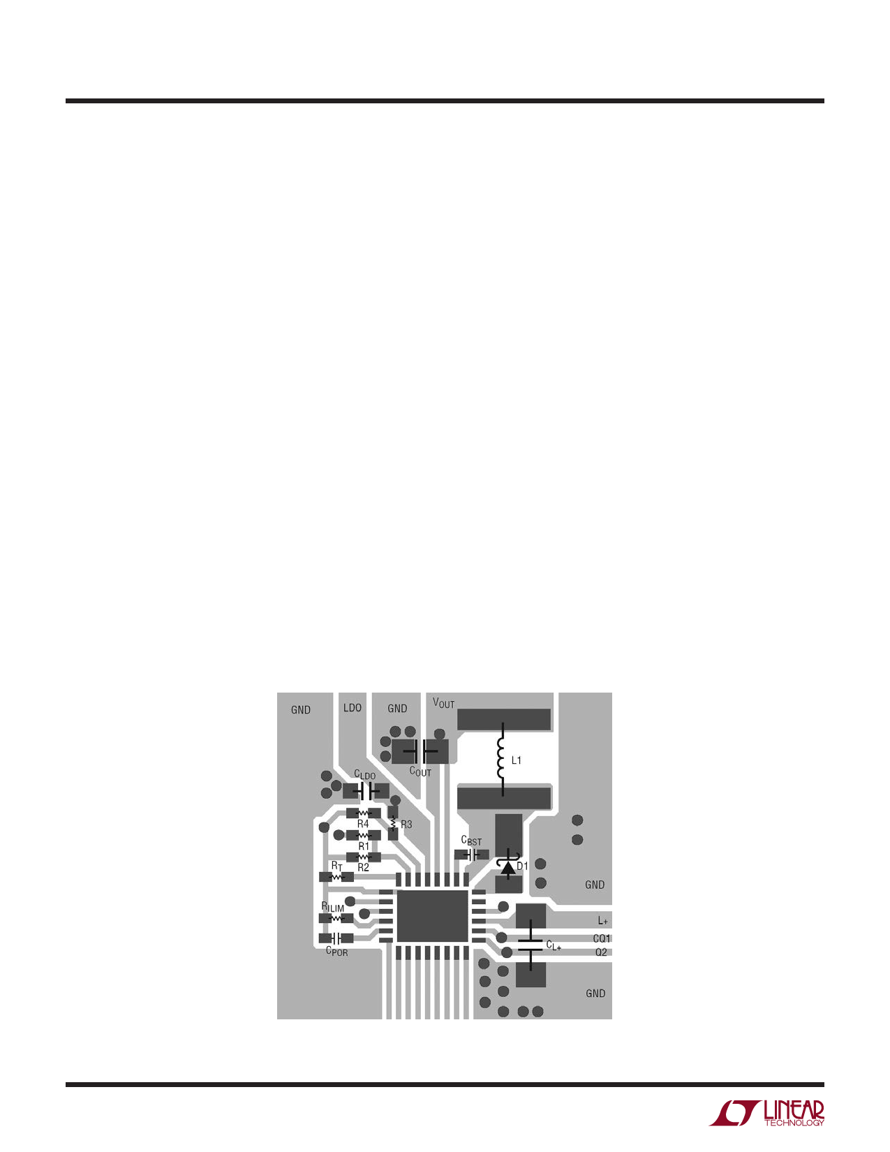
PCB Layout
For proper operation and minimum EMI, care must be taken
during printed circuit board layout. Figure 20 shows the
recommended component placement with trace, ground
plane and via locations. Note that large, switched currents
flow in the LT3669’s L+, SW and GND pins, the external
catch diode (LT3669-2) and the input capacitor (CL+).
Place these components, along with the inductor and
output capacitor (COUT), on the same side of the circuit
board, and connect them on that layer, keeping the loop
they form as small as possible.
All connections to GND should be made at a common star
ground point or directly to a local, unbroken ground plane
underneath. The SW and BST nodes should be laid out
carefully to avoid interference. If the part is synchronized
externally using the SYNC pin, arrange this signal to avoid
interference with sensitive nodes, especially FBLDO, FBOUT,
CPOR, ILIM and RT. Finally, keep the FBLDO, FBOUT, CPOR,
ILIM and RT nodes small so that the ground traces will
shield them from the SW and BST nodes. The exposed
pad, Pin 29, on the bottom of the package acts as a heat
sink and must be soldered to the ground node. To keep
thermal resistance low, extend the ground plane as much as
possible and add thermal vias under and near the LT3669
to any additional ground planes within the circuit board
and on the bottom side.
High Temperature Considerations
Power dissipation within the LT3669 can be estimated by
adding the power dissipated by the switching regulator,
LDO and line drivers. The switching regulator’s power dis-
sipation can be obtained from an efficiency measurement.
The LDO’s power dissipation can be extracted simply by
calculating the product between load current and voltage
drop across the LDO pass device. The line drivers’ con-
tribution can be calculated in a similar manner taking the
product of residual voltage and load current for each driver.
Figure 20. A Good PCB Layout Ensures Proper, Low EMI Operation
3669fa
32
For more information www.linear.com/LT3669
Share Link: 