AD9845AJST View Datasheet(PDF) - Analog Devices
Part Name
Description
Manufacturer
AD9845AJST Datasheet PDF : 22 Pages
| |||
AD9845A
CIRCUIT DESCRIPTION AND OPERATION
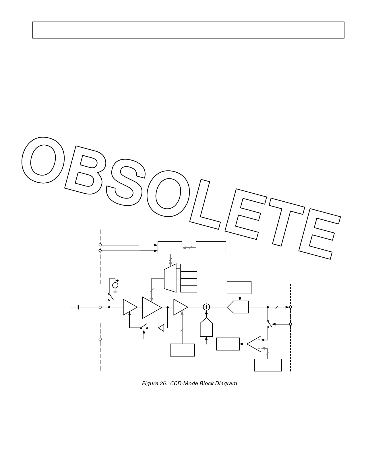
The AD9845A signal processing chain is shown in Figure 25.
Each processing step is essential in achieving a high-quality
image from the raw CCD pixel data.
gain change on the system black level, usually called the “gain
step.” Another advantage of removing this offset at the input
stage is to maximize system headroom. Some area CCDs have
large black level offset voltages, which, if not corrected at the
DC Restore
To reduce the large dc offset of the CCD output signal, a dc-
input stage, can significantly reduce the available headroom in
the internal circuitry when higher VGA gain settings are used.
restore circuit is used with an external 0.1 µF series coupling
capacitor. This restores the dc level of the CCD signal to approxi-
mately 1.5 V, to be compatible with the 3 V single supply of
the AD9845A.
Horizontal timing is shown in Figure 6. It is recommended
that the CLPDM pulse be used during valid CCD dark pixels.
CLPDM may be used during the optical black pixels, either
together with CLPOB or separately. The CLPDM pulse should
Correlated Double Sampler
be a minimum of 4 pixels wide.
The CDS circuit samples each CCD pixel twice to extract the
PxGA
OBSOLETE video information and reject low-frequency noise. The timing
shown in Figure 5 illustrates how the two CDS clocks, SHP
and SHD, are used to sample the reference level and data level
of the CCD signal respectively. The CCD signal is sampled on
the rising edges of SHP and SHD. Placement of these two clock
signals is critical in achieving the best performance from the CCD.
An internal SHP/SHD delay (tID) of 3 ns is caused by internal
propagation delays.
Input Clamp
A line-rate input clamping circuit is used to remove the CCD’s
optical black offset. This offset exists in the CCD’s shielded black
reference pixels. Unlike some AFE architectures, the AD9845A
removes this offset in the input stage to minimize the effect of a
The PxGA provides separate gain adjustment for the individual
color pixels. A programmable gain amplifier with four separate
values, the PxGA has the capability to “multiplex” its gain value
on a pixel-to-pixel basis. This allows lower output color pixels to
be gained up to match higher output color pixels. Also, the PxGA
may be used to adjust the colors for white balance, reducing the
amount of digital processing that is needed. The four different gain
values are switched according to the “Color Steering” circuitry.
Seven different color steering modes for different types of CCD
color filter arrays are programmed in the AD984x’s Control Regis-
ter. For example, Mosaic Separate steering mode accommodates
the popular “Bayer” arrangement of Red, Green, and Blue filters
(see Figure 26).
VD
COLOR
3
PxGA MODE
HD
STEERING
SELECTION
2
0.1F
CCDIN
DC RESTORE
6
CDS
PxGA
4:1
MUX
GAIN0
GAIN1
GAIN2
GAIN3
PxGA GAIN
REGISTERS
2dB TO 36dB
VGA
INTERNAL
VREF
2V FULL SCALE
12-BIT
12
ADC
DOUT
CLPDM
–2dB TO +10dB
INPUT OFFSET
CLAMP
10
VGA GAIN
REGISTER
8-BIT
DAC
OPTICAL BLACK
CLAMP
DIGITAL
FILTERING
8
CLAMP LEVEL
REGISTER
CLPOB
Figure 25. CCD-Mode Block Diagram
REV. 0
–17–
Share Link: 