AD9845AJST View Datasheet(PDF) - Analog Devices
Part Name
Description
Manufacturer
AD9845AJST Datasheet PDF : 22 Pages
| |||
AD9845A
CCD: PROGRESSIVE BAYER
R Gr R Gr LINE0
MOSAIC SEPARATE COLOR
STEERING MODE
GAIN0, GAIN1, GAIN0, GAIN1 ...
Gb B Gb B LINE1
GAIN2, GAIN3, GAIN2, GAIN3 ...
R Gr R Gr LINE2
GAIN0, GAIN1, GAIN0, GAIN1 ...
Gb B Gb B
Figure 26. CCD Color Filter Example: Progressive Scan
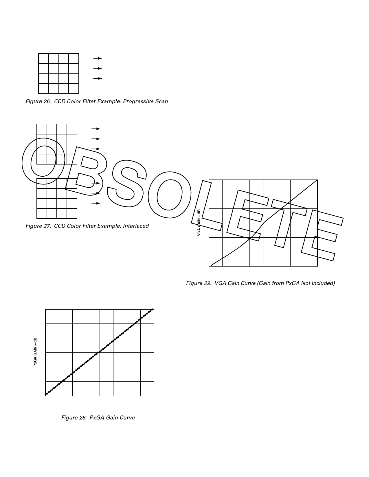
for the AD9845A is 6 dB to 40 dB. The minimum gain of 6 dB
is needed to match a 1 V input signal with the ADC full-scale
range of 2 V. When compared to 1 V full-scale systems (such as
ADI’s AD9803), the equivalent gain range is 0 dB to 34 dB.
The VGA gain curve is divided into two separate regions. When
the VGA Gain Register code is between 0 and 511, the curve
follows a (1 + x)/(1 – x) shape, which is similar to a “linear-in-
dB” characteristic. From code 512 to code 1023, the curve follows
a “linear-in-dB” shape. The exact VGA gain can be calculated
for any Gain Register value by using the following two equations:
CCD: INTERLACED BAYER
EVEN FIELD
VD SELECTED COLOR
STEERING MODE
Code Range Gain Equation (dB)
0–511
Gain = 20 log10 ([658 + code]/[658 – code]) – 0.4
R Gr R Gr LINE0
GAIN0, GAIN1, GAIN0, GAIN1 ...
512 –1023 Gain = (0.0354)(code) – 0.4
OBSOLETE R Gr R Gr LINE1
R Gr R Gr LINE2
R Gr R Gr
GAIN0, GAIN1, GAIN0, GAIN1 ...
GAIN0, GAIN1, GAIN0, GAIN1 ...
ODD FIELD
Gb B Gb B LINE0
GAIN2, GAIN3, GAIN2, GAIN3 ...
Gb B Gb B LINE1
Gb B Gb B LINE2
GAIN2, GAIN3, GAIN2, GAIN3 ...
GAIN2, GAIN3, GAIN2, GAIN3 ...
Gb B Gb B
Figure 27. CCD Color Filter Example: Interlaced
The same Bayer pattern can also be interlaced, and the VD
Selected mode should be used with this type of CCD (see Fig-
As shown in the CCD Mode Specifications, only the VGA gain
range from 2 dB to 36 dB has tested and guaranteed accuracy.
This corresponds to a VGA gain code range of 91 to 1023. The
Gain Accuracy Specifications also include the PxGA gain of 4 dB,
for a total gain range of 6 dB to 40 dB.
36
30
24
18
12
ure 27). The Color Steering performs the proper multiplexing of
the R, G, and B gain values (loaded into the PxGA gain regis-
6
ters), and is synchronized by the user with vertical (VD) and
horizontal (HD) sync pulses. For more detailed information, see
0
0
127 255 383 511 639 767 895 1023
the PxGA Timing section. The PxGA gain for each of the four
VGA GAIN REGISTER CODE
channels is variable from –2 dB to +10 dB, controlled in 64 steps
through the serial interface. The PxGA gain curve is shown in
Figure 28.
Figure 29. VGA Gain Curve (Gain from PxGA Not Included)
Optical Black Clamp
The optical black clamp loop is used to remove residual offsets
in the signal chain, and to track low-frequency variations in the
10
CCD’s black level. During the optical black (shielded) pixel
interval on each line, the ADC output is compared with a fixed
8
black level reference, selected by the user in the Clamp Level
Register. Any value between 0 LSB and 255 LSB may be pro-
6
grammed, with 8-bit resolution. The resulting error signal is
filtered to reduce noise, and the correction value is applied to
4
the ADC input through a D/A converter. Normally, the optical
black clamp loop is turned on once per horizontal line, but this
2
loop can be updated more slowly to suit a particular application.
If external digital clamping is used during the post processing,
the AD9845A optical black clamping may be disabled using Bit
0
D5 in the Operation Register (see Serial Interface Timing and
–2
32
40
(100000)
48
56
0
8
16
PxGA GAIN REGISTER CODE
24 31
(011111)
Internal Register Description section). When the loop is disabled,
the Clamp Level Register may still be used to provide program-
mable offset adjustment.
Figure 28. PxGA Gain Curve
Variable Gain Amplifier
The VGA stage provides a gain range of 2 dB to 36 dB, program-
mable with 10-bit resolution through the serial digital interface.
Combined with 4 dB from the PxGA stage, the total gain range
Horizontal timing is shown in Figure 6. The CLPOB pulse
should be placed during the CCD’s optical black pixels. It is
recommended that the CLPOB pulse duration be at least 20
pixels wide to minimize clamp noise. Shorter pulsewidths may be
used, but clamp noise may increase, and the ability to track
low-frequency variations in the black level will be reduced.
–18–
REV. 0
Share Link: 