CY7C1069AV33 View Datasheet(PDF) - Cypress Semiconductor
Part Name
Description
Manufacturer
CY7C1069AV33 Datasheet PDF : 9 Pages
| |||
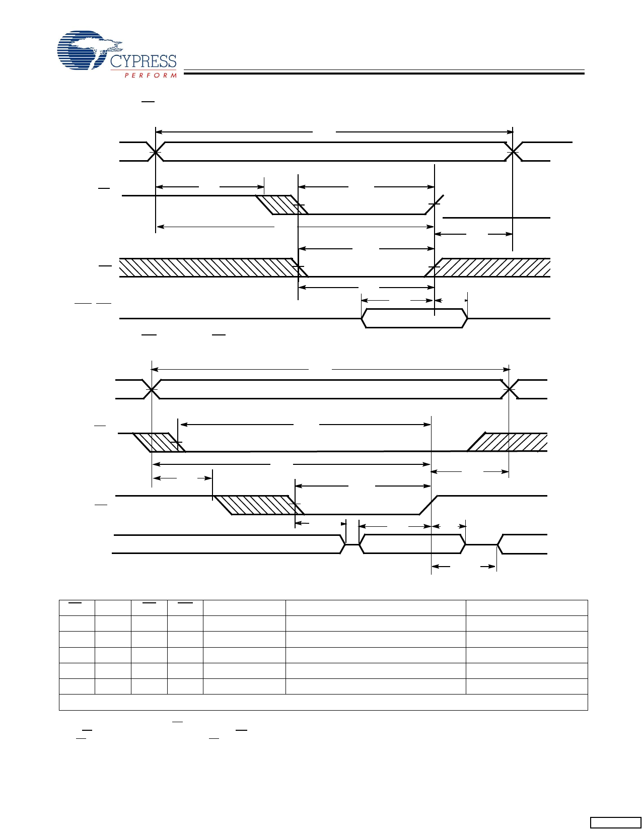
Switching Waveforms (continued)
Write Cycle No. 1 (CE1 Controlled)[16, 17, 18]
tWC
ADDRESS
CY7C1069AV33
CE
tSA
tSCE
tAW
WE
DATAI/O
Write Cycle No. 2 (WE Controlled, OE LOW)[16, 17, 18]
tWC
ADDRESS
tPWE
tBW
tSD
tHA
tHD
CE
tSCE
tSA
WE
DATA I/O
tAW
tPWE
tHZWE
tSD
Truth Table
CE1 CE2 OE WE
I/O0–I/O7
H
X
X
X High-Z
X
L
X
X High-Z
L
H
L
H Data Out
L
H
X
L Data In
L
H
H
H High-Z
Mode
Power-down
Power-down
Read All Bits
Write All Bits
Selected, Outputs Disabled
tHA
tHD
tLZWE
Power
Standby (ISB)
Standby (ISB)
Active (ICC)
Active (ICC)
Active (ICC)
Notes:
16. Data I/O is high-impedance if OE = VIH.
17. If CE1 goes HIGH/CE2 LOW simultaneously with WE going HIGH, the output remains in a high–impedance state.
18. CE above is defined as a combination of CE1 and CE2. It is active low.
Document #: 38-05255 Rev. *F
Page 6 of 9
[+] Feedback
Share Link: 