DSP56364UM View Datasheet(PDF) - Motorola => Freescale
Part Name
Description
Manufacturer
DSP56364UM Datasheet PDF : 162 Pages
| |||
Freescale Semiconductor, Inc.
Signal/Connection Descriptions
External Memory Expansion Port (Port A)
1.5.3
External Bus Control
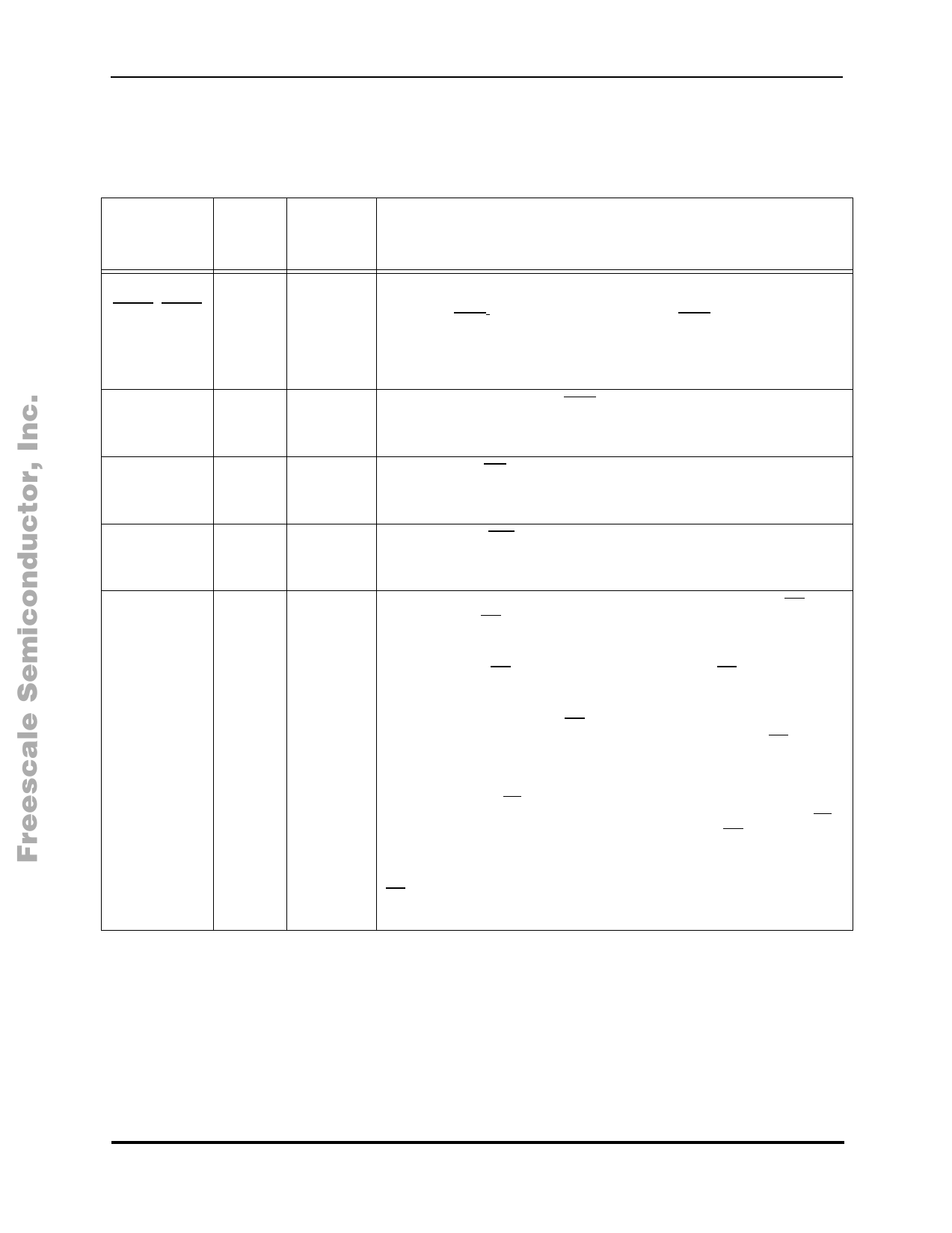
Table 1-7 External Bus Control Signals
Signal Name Type
AA0–AA1/
RAS0–RAS1
Output
CAS
Output
RD
Output
WR
Output
TA
Input
State
during
Reset
Signal Description
Tri-stated
Tri-stated
Tri-stated
Tri-stated
Ignored
Input
Address Attribute or Row Address Strobe—When defined as AA, these
signals can be used as chip selects or additional address lines. When
defined as RAS, these signals can be used as RAS for DRAM interface.
These signals are tri-statable outputs with programmable polarity. These
signals are tri-stated during hardware reset and when the DSP is in the
stop or wait low-power standby mode.
Column Address Strobe— CAS is an active-low output used by DRAM
to strobe the column address. This signal is tri-stated during hardware
reset and when the DSP is in the stop or wait low-power standby mode.
Read Enable—RD is an active-low output that is asserted to read exter-
nal memory on the data bus. This signal is tri-stated during hardware reset
and when the DSP is in the stop or wait low-power standby mode.
Write Enable— WR is an active-low output that is asserted to write exter-
nal memory on the data bus. This signal is tri-stated during hardware reset
and when the DSP is in the stop or wait low-power standby mode.
Transfer Acknowledge—If there is no external bus activity, the TA input
is ignored. The TA input is a data transfer acknowledge (DTACK) function
that can extend an external bus cycle indefinitely. Any number of wait
states (1, 2. . .infinity) may be added to the wait states inserted by the
BCR by keeping TA deasserted. In typical operation, TA is deasserted at
the start of a bus cycle, is asserted to enable completion of the bus cycle,
and is deasserted before the next bus cycle. The current bus cycle com-
pletes one clock period after TA is asserted synchronous to the internal
system clock. The number of wait states is determined by the TA input or
by the bus control register (BCR), whichever is longer. The BCR can be
used to set the minimum number of wait states in external bus cycles.
In order to use the TA functionality, the BCR must be programmed to at
least one wait state. A zero wait state access cannot be extended by TA
deassertion, otherwise improper operation may result. TA can operate
synchronously or asynchronously, depending on the setting of the TAS bit
in the operating mode register (OMR).
TA functionality may not be used while performing DRAM type accesses,
otherwise improper operation may result.
MOTOROLA
DSP56364 Advance Information
1-7
For More Information On This Product,
Go to: www.freescale.com
Share Link: 