DSP56100 View Datasheet(PDF) - Motorola => Freescale
Part Name
Description
Manufacturer
DSP56100 Datasheet PDF : 63 Pages
| |||
PRELIMINARY - 6/15/93
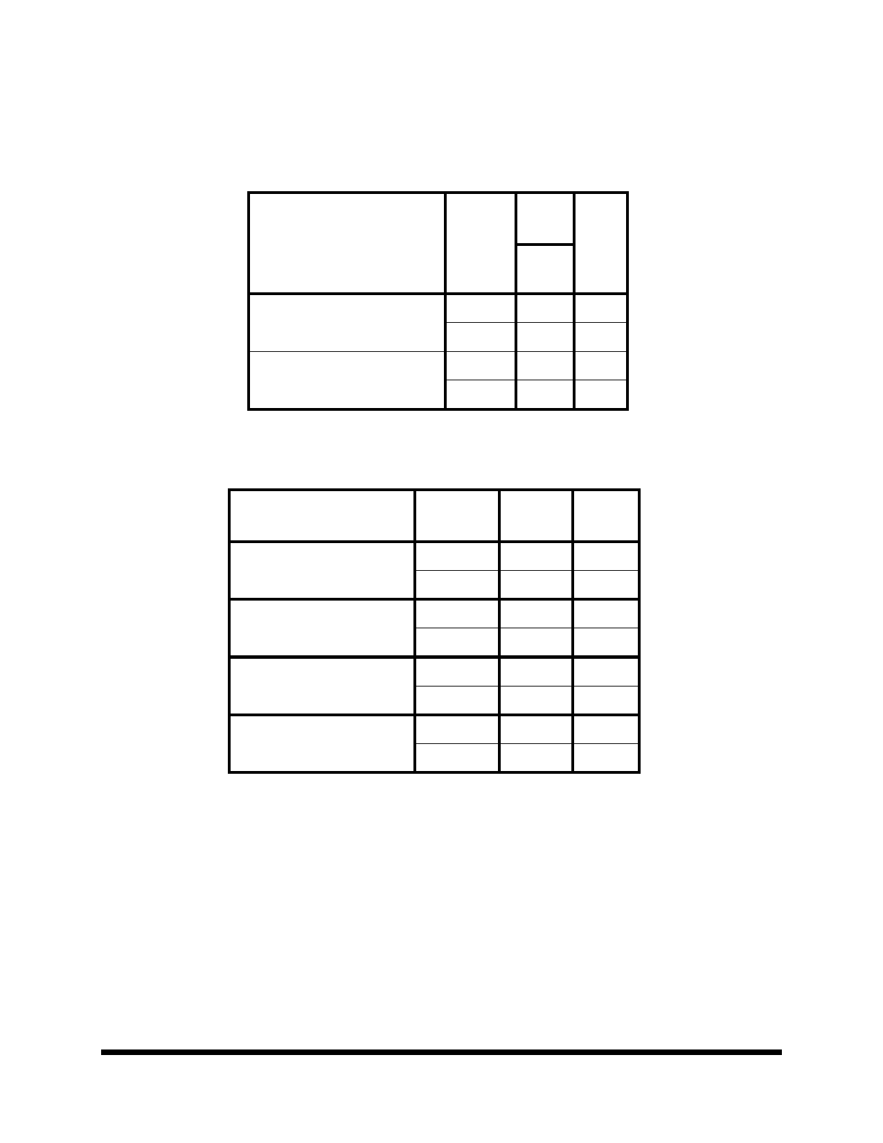
Power Dissipation
(Vdd = 5.0 Vdc +/- 10%, TJ = -40 to +125 °C, CL = 50 pF + 1 TTL Load).
The DC electrical characteristics of this device are shown below.
Conditions
Symbol
Typic
al(5V)
60
MHz
Unit
Digital Vdd with
Codec & PLL disabled
IDD
100 mA
PD
500 mW
Digital Vdd WAIT Mode with IDD
CODEC & PLL disabled
PD
11 mA
55 mW
Conditions
STOP Mode with
PLL and CLKO disabled
Digital current drawn by
the PLL when active
Analog Vdd with
CODEC enabled
Analog Vdd with
CODEC disabled
Symbol
Typical
(5V)
Unit
IDD
400
µA
PD
2
mW
IDD
2
mA
PD
10
mW
IDDA
10
mA
PDA
20
mW
IDDA
PDA
75
µA
375
µW
In order to minimize the power dissipation, all unused digital inputs pins should be tied inactive to VDD or
Vss and all unused I/O pins should be tied inactive through a 10KΩ resistor to VDD or Vss. All port A input
pins and bydirectional pins must have a valid state at all time when port A is released in order to minimize
power; those pins must then be pulled up or down or driven by another device.
When the codec is not used, VDDA should be connected to VDD and VssA to Vss, and all codec pins should
be left floating except Vref which should still be decoupled.
5
DSP56166 Technical Data Sheet
MOTOROLA
Share Link: 