DSP56303UM View Datasheet(PDF) - Freescale Semiconductor
Part Name
Description
Manufacturer
DSP56303UM Datasheet PDF : 108 Pages
| |||
Specifications
Table 2-7. Reset, Stop, Mode Select, and Interrupt Timing6 (Continued)
No.
Characteristics
Expression
100 MHz
Unit
Min Max
Notes: 1. When fast interrupts are used and IRQA, IRQB, IRQC, and IRQD are defined as level-sensitive, timings 19 through 21 apply to
prevent multiple interrupt service. To avoid these timing restrictions, the deasserted Edge-triggered mode is recommended
when fast interrupts are used. Long interrupts are recommended for Level-sensitive mode.
2. This timing depends on several settings:
• For PLL disable, using internal oscillator (PLL Control Register (PCTL) Bit 16 = 0) and oscillator disabled during Stop (PCTL
Bit 17 = 0), a stabilization delay is required to assure that the oscillator is stable before programs are executed. Resetting the
Stop delay (Operating Mode Register Bit 6 = 0) provides the proper delay. While Operating Mode Register Bit 6 = 1 can be set,
it is not recommended, and these specifications do not guarantee timings for that case.
• For PLL disable, using internal oscillator (PCTL Bit 16 = 0) and oscillator enabled during Stop (PCTL Bit 17=1), no
stabilization delay is required and recovery is minimal (Operating Mode Register Bit 6 setting is ignored).
• For PLL disable, using external clock (PCTL Bit 16 = 1), no stabilization delay is required and recovery time is defined by the
PCTL Bit 17 and Operating Mode Register Bit 6 settings.
• For PLL enable, if PCTL Bit 17 is 0, the PLL is shutdown during Stop. Recovering from Stop requires the PLL to get locked.
The PLL lock procedure duration, PLL Lock Cycles (PLC), may be in the range of 0 to 1000 cycles. This procedure occurs in
parallel with the stop delay counter, and stop recovery ends when the last of these two events occurs. The stop delay counter
completes count or PLL lock procedure completion.
• PLC value for PLL disable is 0.
• The maximum value for ETC is 4096 (maximum MF) divided by the desired internal frequency (that is, for 66 MHz it is 4096/66
MHz = 62 µs). During the stabilization period, TC, TH, and TL is not constant, and their width may vary, so timing may vary as
well.
3. Periodically sampled and not 100 percent tested.
4. Value depends on clock source:
• For an external clock generator, RESET duration is measured while RESET is asserted, VCC is valid, and the EXTAL input is
active and valid.
• For an internal oscillator, RESET duration is measured while RESET is asserted and VCC is valid. The specified timing
reflects the crystal oscillator stabilization time after power-up. This number is affected both by the specifications of the crystal
and other components connected to the oscillator and reflects worst case conditions.
• When the VCC is valid, but the other “required RESET duration” conditions (as specified above) have not been yet met, the
device circuitry is in an uninitialized state that can result in significant power consumption and heat-up. Designs should
minimize this state to the shortest possible duration.
5. If PLL does not lose lock.
6. VCC = 3.3 V ± 0.3 V; TJ = –40°C to +100°C, CL = 50 pF.
7. WS = number of wait states (measured in clock cycles, number of TC).
8. Use the expression to compute a maximum value.
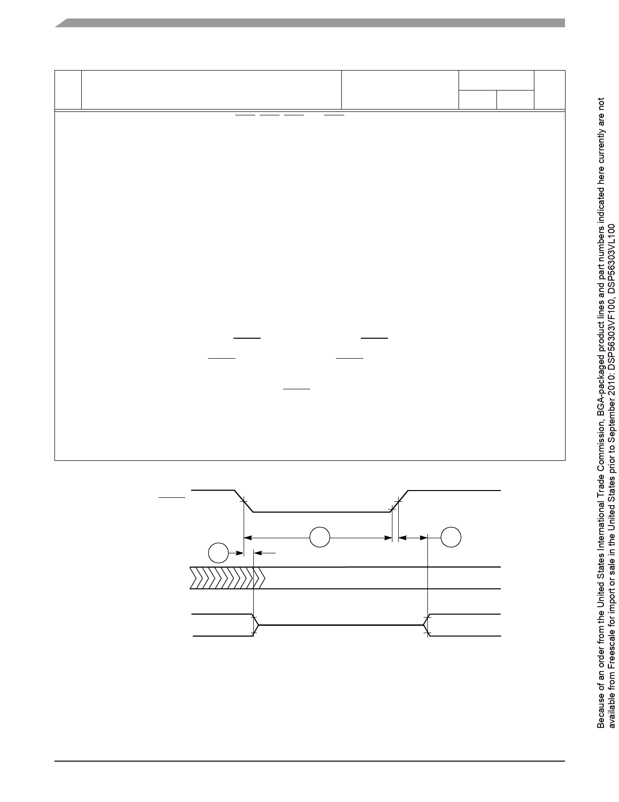
VIH
RESET
9
10
8
All Pins
Reset Value
A[0–17]
Figure 2-3. Reset Timing
First Fetch
DSP56303 Technical Data, Rev. 11
2-8
Freescale Semiconductor
Share Link: 