DSP56311 View Datasheet(PDF) - Freescale Semiconductor
Part Name
Description
Manufacturer
DSP56311 Datasheet PDF : 96 Pages
| |||
1.12 JTAG and OnCE Interface
JTAG and OnCE Interface
The DSP56300 family and in particular the DSP56311 support circuit-board test strategies based on the IEEE®
Std. 1149.1™ test access port and boundary scan architecture, the industry standard developed under the
sponsorship of the Test Technology Committee of IEEE and the JTAG. The OnCE module provides a means to
interface nonintrusively with the DSP56300 core and its peripherals so that you can examine registers, memory, or
on-chip peripherals. Functions of the OnCE module are provided through the JTAG TAP signals. For programming
models, see the chapter on debugging support in the DSP56300 Family Manual.
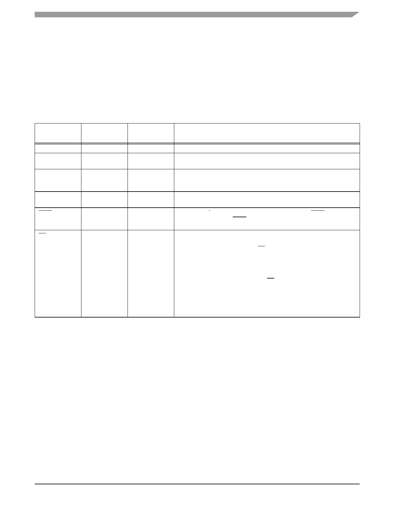
Table 1-16. JTAG/OnCE Interface
Signal
Name
TCK
TDI
TDO
TMS
TRST
DE
Type
Input
Input
Output
Input
Input
Input/ Output
State During
Reset
Input
Input
Tri-stated
Input
Input
Input
Signal Description
Test Clock—A test clock input signal to synchronize the JTAG test logic.
Test Data Input—A test data serial input signal for test instructions and data.
TDI is sampled on the rising edge of TCK and has an internal pull-up resistor.
Test Data Output—A test data serial output signal for test instructions and
data. TDO is actively driven in the shift-IR and shift-DR controller states. TDO
changes on the falling edge of TCK.
Test Mode Select—Sequences the test controller’s state machine. TMS is
sampled on the rising edge of TCK and has an internal pull-up resistor.
Test Reset—Initializes the test controller asynchronously. TRST has an
internal pull-up resistor. TRST must be asserted during and after power-up
(see EB610/D for details).
Debug Event—As an input, initiates Debug mode from an external command
controller, and, as an open-drain output, acknowledges that the chip has
entered Debug mode. As an input, DE causes the DSP56300 core to finish
executing the current instruction, save the instruction pipeline information,
enter Debug mode, and wait for commands to be entered from the debug
serial input line. This signal is asserted as an output for three clock cycles
when the chip enters Debug mode as a result of a debug request or as a result
of meeting a breakpoint condition. The DE has an internal pull-up resistor.
This signal is not a standard part of the JTAG TAP controller. The signal
connects directly to the OnCE module to initiate debug mode directly or to
provide a direct external indication that the chip has entered Debug mode. All
other interface with the OnCE module must occur through the JTAG port.
Freescale Semiconductor
DSP56311 Technical Data, Rev. 8
1-15
Share Link: 