DSP56362 View Datasheet(PDF) - Freescale Semiconductor
Part Name
Description
Manufacturer
DSP56362 Datasheet PDF : 152 Pages
| |||
Thermal Characteristics
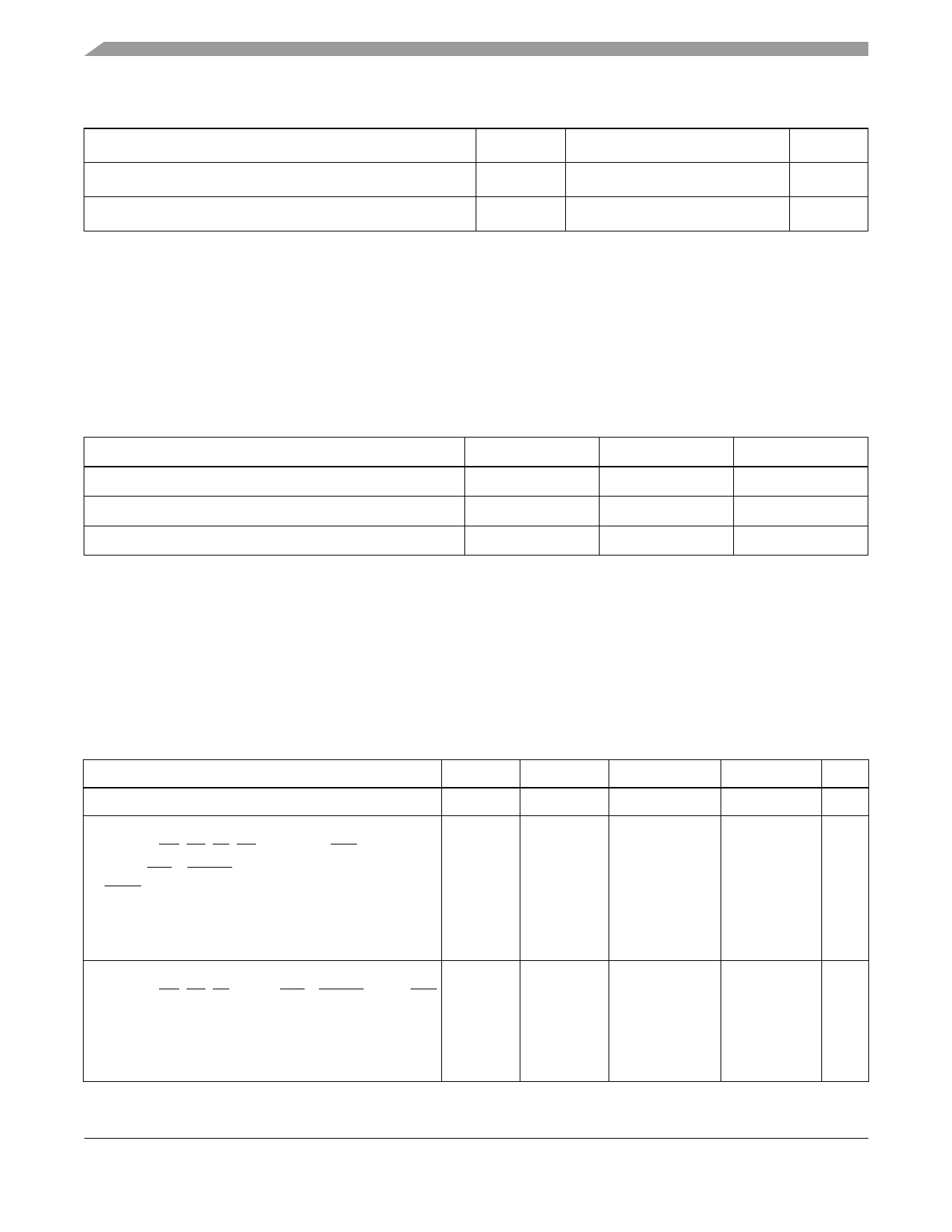
Table 3-1 Maximum Ratings (continued)
Rating1
Symbol
Value1, 2
Unit
Operating temperature range
TJ
−40 to +105
°C
Storage temperature
TSTG
−55 to +125
°C
1 GND = 0 V, VCC = 3.3 V ± .16 V, TJ = 0°C to +100°C, CL = 50 pF
2 Absolute maximum ratings are stress ratings only, and functional operation at the maximum is not guaranteed. Stress beyond
the maximum rating may affect device reliability or cause permanent damage to the device.
3 CAUTION: All “5 V Tolerant” input voltages must not be more than 3.95 V greater than the supply voltage; this restriction
applies to “power on”, as well as during normal operation. In any case, the input voltages cannot be more than 5.75 V. “5 V
Tolerant” inputs are inputs that tolerate 5 V.
3.3 Thermal Characteristics
Table 3-2 Thermal Characteristics
Characteristic
Symbol
LQFP Value
Unit
Junction-to-ambient thermal resistance1
Junction-to-case thermal resistance2
RθJA or θJA
RθJC or θJC
45.3
10.1
°C/W
°C/W
Thermal characterization parameter
ΨJT
5.5
°C/W
1 Junction-to-ambient thermal resistance is based on measurements on a horizontal single-sided printed circuit board per SEMI
G38-87 in natural convection.(SEMI is Semiconductor Equipment and Materials International, 805 East Middlefield Rd.,
Mountain View, CA 94043, (415) 964-5111.
Measurements were done with parts mounted on thermal test boards conforming to specification EIA/JESD51-3.
2 Junction-to-case thermal resistance is based on measurements using a cold plate per SEMI G30-88, with the exception that
the cold plate temperature is used for the case temperature.
3.4 DC Electrical Characteristics
Table 3-3 DC Electrical Characteristics1
Characteristics
Symbol
Min
Typ
Supply voltage
VCC
3.14
3.3
Input high voltage
• D(0:23), BG, BB, TA, DE, and PINIT/NMI
• MOD2/IRQ2, RESET, and TCK/TDI/TMS/
TRST/ESAI/Timer/HDI08/ SHI(SPI mode) pins
• SHI(I2C mode) pins
• EXTAL3
VIH
2.0
—
VIHP
2.0
—
1.5
VIHX
0.8 × VCC
—
Input low voltage
• D(0:23), BG, BB, TA, MOD2/IRQ2, RESET, PINIT/NMI
VIL
–0.3
—
• All JTAG/ESAI/Timer/HDI08/ SHI(SPI mode) pins
VILP
–0.3
—
• SHI(I2C mode) pins
• EXTAL3
–0.3
—
VILX
–0.3
Max
3.46
VCC
VCC + 3.95
Unit
V
V
VCC + 3.95
VCC
V
0.8
0.8
0.3 × VCC
0.2 × VCC
DSP56362 Technical Data, Rev. 4
3-2
Freescale Semiconductor
Share Link: 