FAN7585 View Datasheet(PDF) - Fairchild Semiconductor
Part Name
Description
Manufacturer
FAN7585 Datasheet PDF : 16 Pages
| |||
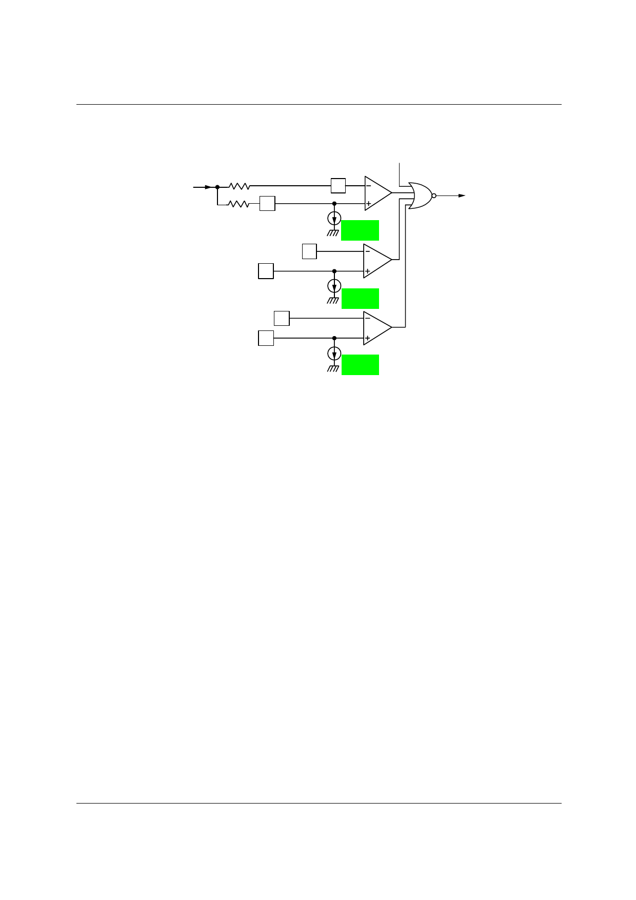
3. OCP Block
FAN7585
Sense Inductor
Equivalent Resistor(Rs) ≅ 5mΩ
Io
17
Roffset IS12
(Offset Voltage Resistor)
VS12
18
OVP Outpu t
COMP1
IrIeref1f × 5
VS5
(100uA)
16
IS5 15
VS33 14
COMP2
IrIeref1f ×× 5
(100uA)
IS33 13
COMP3
IrIeref1f ×× 5
(100uA)
Iref1=20µA at RI=62kΩ
TPROT
It also has OCP function for +3.3V,+5V,+12V outputs. The block is made up of three comparators. Pin17(IS12), pin15(IS5)
and pin13(IS33) are current sense inputs for +12V, +5V and +3.3V outputs respectively. These pins are connected to the cur-
rent sensing resistor or inductor.
Each OCP level is determined by RI resistor , so you can define over current protection level by changing RI resistor. Pin8(RI)
voltage is always 1.25V, so if you connect 62kΩ resistor, the reference current is 20uA(Iref1).
If the voltage drop of the sense resistor or inductor is larger than offset voltage (Voffset = Roffset × 5 × Iref1), the DTC becomes
"High" after some delay(38ms at CTUVP=0.47uF)and the main SMPS is turned off. That means the output voltage(+3.3V,
+5V, +12V) will be ground level.
After main power is turned off at OCP and initialized by REM, if REM signal is changed from "High" to "Low", main power
becomes operational.
For example, if you want to define 5V output OCP level at 10A in the condition of equivalent resistor(Rs)= 5mΩ, you can
determine the offset voltage resistor(Roffset) as following method.
- Iref1 = 1.25V / 62kΩ = 20uA
- Voffset = RS × 5 × Iref1 = 5mΩ × 10A = 50mV
- Therefore, Roffset = 50mV / (5 × Iref1) = 500Ω
By the way, OCP output signal can be delayed by protection delay capacitor(CTUVP) and its delay time is decided by the value
of CTUVP.
Tuvp
≈
C-----T---U----V∆---P-I---*---∆----V--
=
0----.--4---7----u---F----*---1---.--7----V--
21uA
=
38msec
If you use too small (or large) capacitor, the charging time would decrease (or increase) very much and it can cause
malfunction at the transient time. So you have to choose the reasonable delay time for system optimization by changing the
external capacitor value.
11
Share Link: 