LC66E516 View Datasheet(PDF) - SANYO -> Panasonic
Part Name
Description
Manufacturer
LC66E516 Datasheet PDF : 18 Pages
| |||
LC66E516
Specifications
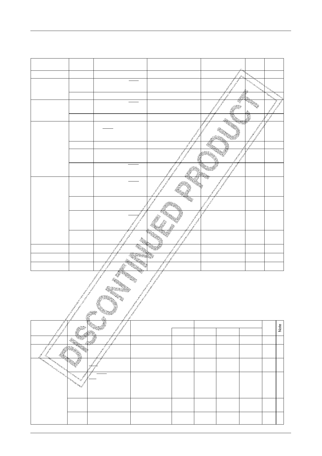
Absolute Maximum Ratings at Ta = 25˚C, VSS=0V
Parameter
Symbol
Pins applicable and related
information
Supply voltage
Input voltage
Output voltage
VDD
VIN(1)
VIN(2)
VOUT(1)
VOUT(2)
ION(1)
VDD
P2, P3 (except P33/HOLD)
and P6.
All the pins other than the
above
P2,P 3 (except P33/HOLD),
P6, P7 and PA.
All the pins other than the
above.
P0, P1, P2, P3 ( except
P33/HOLD), P4, P5, P6,P8,P9
and PC.
Output current per
pin
ION(2) P7, PA, PB
–IOP(1) P0, P1, P4, P5, P7, PA, PB
P2, P3 (except P33/HOLD),
–IOP(2) P6, P8, P9 and PC.
∑ION(1)
P2, P3 (except P33/HOLD),
P4, P5, P6, P7 and P8.
Conditions
Ratings
Unit
–0.3 to +7.0 V
–0.3 to +15.0 V
–0.2 to VDD+0.3
V
–0.3 to +15.0 V
–0.3 to VDD+0.3
V
4 mA
Note
1
2
1
2
3
20 mA
3
2 mA
4
4 mA
4
75 mA
3
Pin total current
∑ION(2) P0, P1, P9, PA, PB, PC
–∑IOP(1)
P2, P3 (except P33/HOLD),
P4, P5, P6, P7 and P8.
75 mA
3
25 mA
4
–∑IOP(2) P0, P1, P9, PA, PB, PC
25 mA
4
Allowable power
dissipation
Operating
temperature
Storage temperature
Pd max
Topr
Tstg
Ta=10 to 40°C
DIC-64S
600 mW
10 to 40 °C
–55 to +125 °C
Note 1: Applicable only to the pins with open drain output circuit. Otherwise, refer to the values listed in the "all the pins
other than the above" column.
Note 2: As far as oscillation input and output are concerned, the voltage range can cover the self-oscillating level.
Note 3: Sink current. As far as the P8 is concerned, these parameters can apply only to the CMOS output circuit.
Note 4: Source current. Apply to the both of the pull-up output circuit and the CMOS output circuit except for P8.
Allowable operating conditions at Ta = 10˚C to 40°C, VSS=0V, unless otherwise noted
Parameter
Operating supply
voltage
Memory backup
voltage
symbol
Pins applicable
VDD VDD
VDD(H) VDD
Conditions
With HOLD mode
"ON"
VDD(V)
min
4.5
Ratings
typ
5.0
1.8
Unit
max
5.5 V
5.5 V
Input high-level
voltage
P2, P3(except P33/
VIH(1) HOLD) and P6.
VIH(2)
P33/HOLD, P9
RES
VIH(3)
OSC1
PO, P1, P4, P5, PC,
PD, PE
VIH(4) PE
With output Nch
transistor "OFF"
With output Nch
transistor "OFF"
With output Nch
transistor "OFF"
With tristate input
mode selected
4.5 to 5.5 0.75VDD
4.5 to 5.5 0.75VDD
4.5 to 5.5
4.5 to 5.5
0.7VDD
0.8VDD
+13.5 V 1
VDD V 2
VDD V 3
VDD V
Continued on next page.
No.2928–11/18
Share Link: 