K4B1G0446D View Datasheet(PDF) - Samsung
Part Name
Description
Manufacturer
K4B1G0446D Datasheet PDF : 60 Pages
| |||
K4B1G04(08/16)46D
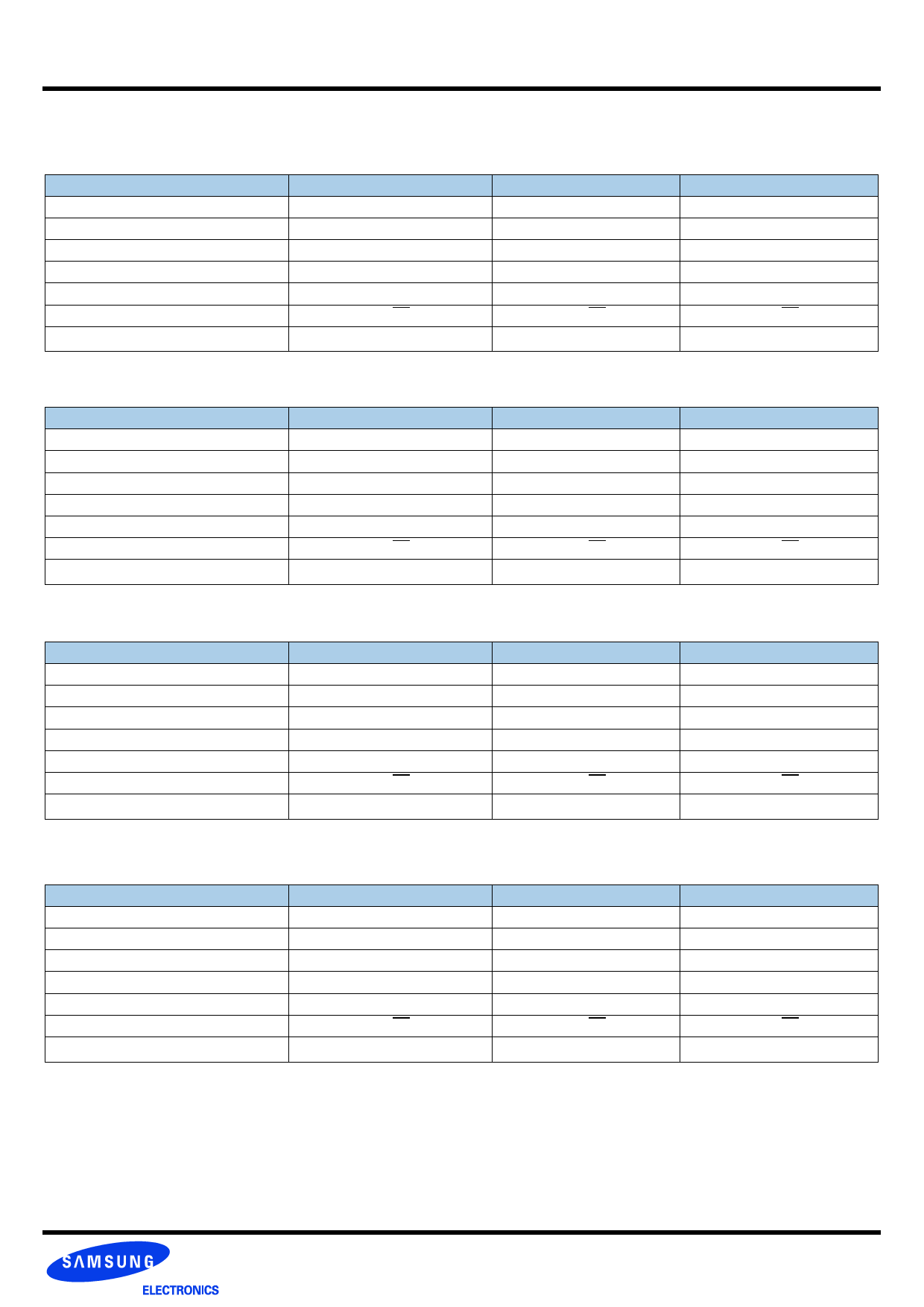
5.0 DDR3 SDRAM Addressing
1Gb
Configuration
# of Bank
Bank Address
Auto precharge
Row Address
Column Address
BC switch on the fly
Page size *1
2Gb
Configuration
# of Bank
Bank Address
Auto precharge
Row Address
Column Address
BC switch on the fly
Page size *1
4Gb
Configuration
# of Bank
Bank Address
Auto precharge
Row Address
Column Address
BC switch on the fly
Page size *1
256Mb x 4
8
BA0 - BA2
A10/AP
A0 - A13
A0 - A9,A11
A12/BC
1 KB
512Mb x 4
8
BA0 - BA2
A10/AP
A0 - A14
A0 - A9,A11
A12/BC
1 KB
1Gb x 4
8
BA0 - BA2
A10/AP
A0 - A15
A0 - A9,A11
A12/BC
1 KB
1Gb DDR3 SDRAM
128Mb x 8
8
BA0 - BA2
A10/AP
A0 - A13
A0 - A9
A12/BC
1 KB
256Mb x 8
8
BA0 - BA2
A10/AP
A0 - A14
A0 - A9
A12/BC
1 KB
512Mb x 8
8
BA0 - BA2
A10/AP
A0 - A15
A0 - A9
A12/BC
1 KB
64Mb x 16
8
BA0 - BA2
A10/AP
A0 - A12
A0 - A9
A12/BC
2 KB
128Mb x 16
8
BA0 - BA2
A10/AP
A0 - A13
A0 - A9
A12/BC
2 KB
256Mb x 16
8
BA0 - BA2
A10/AP
A0 - A14
A0 - A9
A12/BC
2 KB
8Gb
Configuration
# of Bank
Bank Address
Auto precharge
Row Address
Column Address
BC switch on the fly
Page size *1
2Gb x 4
8
BA0 - BA2
A10/AP
A0 - A15
A0 - A9,A11,A13
A12/BC
2 KB
1Gb x 8
8
BA0 - BA2
A10/AP
A0 - A15
A0 - A9,A11
A12/BC
2 KB
512Mb x 16
8
BA0 - BA2
A10/AP
A0 - A15
A0 - A9
A12/BC
2 KB
Note 1 : Page size is the number of bytes of data delivered from the array to the internal sense amplifiers when an ACTIVE command is registered.
Page size is per bank, calculated as follows:
page size = 2 COLBITS * ORG÷8
where, COLBITS = the number of column address bits, ORG = the number of I/O (DQ) bits
Page 12 of 60
Rev. 1.1 August 2008
Share Link: 