K4T1G044QQ View Datasheet(PDF) - Samsung
Part Name
Description
Manufacturer
K4T1G044QQ Datasheet PDF : 44 Pages
| |||
K4T1G044QQ
K4T1G084QQ
K4T1G164QQ
DDR2 SDRAM
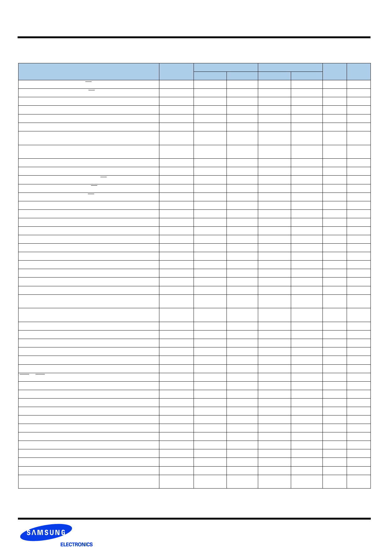
13.3 Timing Parameters by Speed Grade
(Refer to notes for informations related to this table at the bottom)
Parameter
DQ output access time from CK/CK
DQS output access time from CK/CK
CK high-level width
CK low-level width
CK half period
Clock cycle time, CL=x
DQ and DM input hold time
Symbol
tAC
tDQSCK
tCH
tCL
tHP
tCK
tDH(base)
DQ and DM input setup time
Control & Address input pulse width for each input
DQ and DM input pulse width for each input
Data-out high-impedance time from CK/CK
DQS low-impedance time from CK/CK
DQ low-impedance time from CK/CK
DQS-DQ skew for DQS and associated DQ signals
DQ hold skew factor
DQ/DQS output hold time from DQS
First DQS latching transition to associated clock edge
DQS input high pulse width
DQS input low pulse width
DQS falling edge to CK setup time
DQS falling edge hold time from CK
Mode register set command cycle time
Write postamble
Write preamble
Address and control input hold time
tDS(base)
tIPW
tDIPW
tHZ
tLZ(DQS)
tLZ(DQ)
tDQSQ
tQHS
tQH
tDQSS
tDQSH
tDQSL
tDSS
tDSH
tMRD
tWPST
tWPRE
tIH(base)
Address and control input setup time
tIS(base)
Read preamble
Read postamble
Active to active command period for 1KB page size products
Active to active command period for 2KB page size products
Four Activate Window for 1KB page size products
Four Activate Window for 2KB page size products
CAS to CAS command delay
Write recovery time
Auto precharge write recovery + precharge time
Internal write to read command delay
Internal read to precharge command delay
Exit self refresh to a non-read command
Exit self refresh to a read command
Exit precharge power down to any non-read command
Exit active power down to read command
Exit active power down to read command (slow exit, lower power)
CKE minimum pulse width (high and low pulse width)
ODT turn-on delay
ODT turn-on
tRPRE
tRPST
tRRD
tRRD
tFAW
tFAW
tCCD
tWR
tDAL
tWTR
tRTP
tXSNR
tXSRD
tXP
tXARD
tXARDS
tCKE
tAOND
tAON
DDR2-800
min
max
- 400
400
- 350
350
0.45
0.55
0.45
0.55
min(tCL,tCH)
x
2500
8000
125
x
DDR2-667
min
max
-450
+450
-400
+400
0.45
0.55
0.45
0.55
min(tCL, tCH)
x
3000
8000
175
x
50
0.6
0.35
x
tAC min
2* tAC min
x
x
tHP - tQHS
- 0.25
0.35
0.35
0.2
0.2
2
0.4
0.35
250
x
x
x
tAC max
tAC max
tAC max
200
300
x
0.25
x
x
x
x
x
0.6
x
x
100
0.6
0.35
x
tAC min
2*tAC min
x
x
tHP - tQHS
-0.25
0.35
0.35
0.2
0.2
2
0.4
0.35
275
x
x
x
tAC max
tAC max
tAC max
240
340
x
0.25
x
x
x
x
x
0.6
x
x
175
0.9
0.4
7.5
10
35
45
2
15
WR+tRP
7.5
7.5
tRFC + 10
200
2
2
8 - AL
3
2
tAC(min)
x
1.1
0.6
x
x
x
x
x
x
x
x
2
tAC(max) +
0.7
200
x
0.9
1.1
0.4
0.6
7.5
x
10
x
37.5
50
2
15
x
WR+tRP
x
7.5
x
7.5
tRFC + 10
200
2
x
2
x
7 - AL
3
2
2
tAC(min) tAC(max)+0.7
Units
ps
ps
tCK
tCK
ps
ps
ps
ps
tCK
tCK
ps
ps
ps
ps
ps
ps
tCK
tCK
tCK
tCK
tCK
tCK
tCK
tCK
ps
ps
tCK
tCK
ns
ns
ns
ns
tCK
ns
tCK
ns
ns
ns
tCK
tCK
tCK
tCK
tCK
tCK
ns
Notes
20,21
24
15,16,
17,20
15,16,
17,21
27
27
22
21
19
14,16,18,
23
14,16,18,
22
28
28
12
12
23
33
11
9
9, 10
36
13, 25
19 of 44
Rev. 1.01 November 2007
Share Link: 