MP7680 View Datasheet(PDF) - Exar Corporation
Part Name
Description
Manufacturer
MP7680 Datasheet PDF : 12 Pages
| |||
MP7680
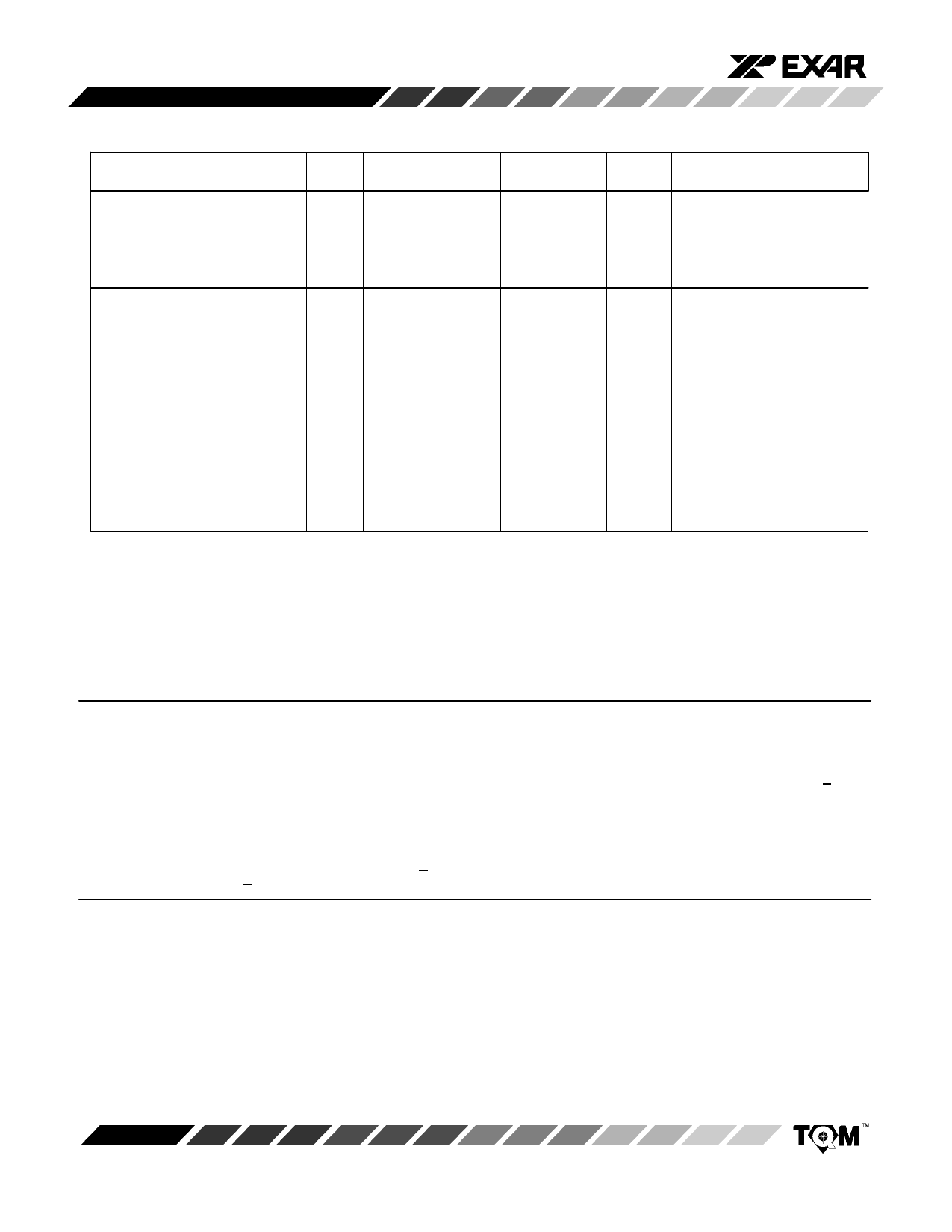
ELECTRICAL CHARACTERISTICS
(CONT’D)
Parameter
POWER SUPPL Y 4
25 °C
Symbol Min
Typ Max
Functional Voltage Range
VDD
4.5
5.5
Supply Current
IDD
2
1
TIMING CHARACTERISTICS
2, 3
Write Pulse Width
Chip Select Set-Up Time
Address Set-Up Time
Chip Select and Address Hold
Time
tWR
75
tCS 100
tAS 100
tH
0
Latch Select Set-Up Time
Latch Select Hold Time
Data Valid Set-Up Time
Data Valid Hold Time
Transfer Pulse Width
Write Cycle (per DAC)
tBS 120
tBH
10
tDS 100
tDH
0
tXFER
65
tWC 175
Tmin to Tmax
Min
Max
Units
4.5
5.5 V
2 mA
1 mA
85
ns
120
ns
120
ns
0
ns
150
ns
15
ns
120
ns
0
ns
75
ns
200
ns
Test Conditions/Comments
Digital inputs = VIL or VIH
Digital inputs = 0 or 5 V
Notes:
1
Full Scale Range (FSR) is 10V for unipolar mode.
2
Guaranteed but not production tested.
3
See timing diagram (Figure 2.).
4
DV D D and AVD D are connected through the silicon substrate. Connect
DC voltage differences will cause undesirable internal currents.
together
at the package.
Specifications are subject to change without notice
ABSOLUTE MAXIMUM RA TINGS (T A = +25 °C unless otherwise noted) 1, 2
VDD to AGND . . . . . . . . . . . . . . . . . . . . . . . . . . . . -0.5 to +7 V
VDD to DGND . . . . . . . . . . . . . . . . . . . . . . . . . . . . -0.5 to +7 V
Digital Input Voltage to DGND . . . . GND -0.5 to VDD +0.5 V
Any IOUT1, IOUT2 to AGND . . . . . . . GND -0.5 to VDD +0.5 V
Any VREF to AGND . . . . . . . . . . . . . . . . . . . . . . . . . . . . +25 V
AGND to DGND . . . . . . . . . . . . . . . . . . . . . . . . . . . . . . . . . +1 V
(Functionality Guaranteed +0.5 V)
Any VRFB to AGND . . . . . . . . . . . . . . . . . . . . . . . . . . . . +25 V
Storage Temperature . . . . . . . . . . . . . . . . . . -65°C to +150°C
Lead Temperature (Soldering, 10 seconds) . . . . . . . +300°C
Package Power Dissipation Rating to 75°C
CDIP, PDIP, PQFP . . . . . . . . . . . . . . . . . . . . . . . . . 800mW
Derates above 75°C . . . . . . . . . . . . . . . . . . . . . 11mW/°C
Notes:
1
Stresses above those listed under “Absolute Maximum Ratings” may cause permanent damage to the device. This is a
stress rating only and functional operation at or above this specification is not implied. Exposure to maximum rating
conditions for extended periods may affect device reliability .
2
Any input pin which can see a value outside the absolute maximum ratings should be protected by Schottky diode clamps
(HP5082-2835) from input pin to the supplies. All inputs have protection diodes which will protect the device from short
transients outside the supplies of less than 100mA for less than 100 ms.
Rev. 3.10
6
Share Link: 