NTE1857 View Datasheet(PDF) - NTE Electronics
Part Name
Description
Manufacturer
NTE1857 Datasheet PDF : 6 Pages
| |||
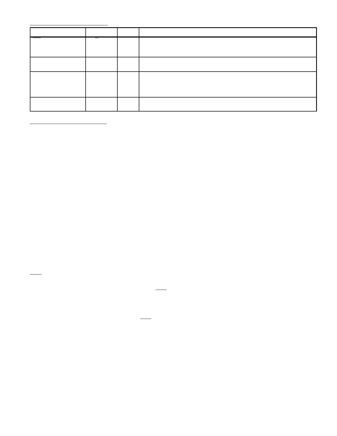
Pin Description (Cont’d):
Name
Symbol
Full/Half Step
F/HS
Clockwise/
Counterclockwise
Output Impedance
Control
CW/CCW
OIC
Phase A
Ph A
Pin #
9
10
8
11
Description
When low (Logic “0”), each clock pulse will cause the motor to rotate one
full step. When high, each clock pulse will cause the motor to rotate one–
half step. See Fig. 1 for sequences.
This input allows reversing the rotation of the motor. See Fig. 1 for se-
quence.
This input is relevant only in the half step mode (Pin9 > 2.0V). When low
(Logic “0”) the two driver outputs of the non–energized coil will be in a high
impedance condition. When high the same driver outputs will be at a low
impedance referenced to VM. See Figure 1.
This open–collector output indicates (when low) that the driver outputs
are in the Phase A condition (L1 = L3 = VOHD, L2 = L4 = VOLD).
Application Information:
General
The NTE1857 integrated circuit is designed to drive a stepper positioning motor in applications such
as disk drives and robotics. The outputs can provide up to 350mA to each of two coils of a two–phase
motor. The outputs change state with each low–to–high transition of the clock input, with the new
output state depending on the previous state, as well as the input conditions on Pins 8, 9, and 10.
Outputs (Pins 2, 3, 14, 15)
The outputs (L1–L4) are high current outputs, which when connected to a two–phase motor, provide
two full–bridge configurations. The polarities applied to the motor coils depend on which transistor
(QH or QL) of each output is on, which in turn depends on the inputs and the decoding circuitry.
The maximum sink current available at the outputs is a function of the resistor connected between
Pin6 and GND (see section on Bias/Set operation). Whenever the outputs are to be in a high imped-
ance state, both transistors (QH and QL) of each output are off.
VD (Pin1)
This pin allows for provision of a current path for the motor coil current during switching, in order to
suppress back–EMF voltage spikes. Pin1 is normally connected to VM (Pin16) through a diode (zener
or regular), a resistor, or directly. The peak instantaneous voltage at the outputs (Pins 2, 3, 14, and
15) must not exceed VM by more than 6 volts. The voltage drop across the internal clamping diodes
must be included in design. Parasitic diodes across each QL of each output provide for a complete
circuit path for the switched current.
Full/Half Step (Pin9)
When this input is at a Logic “0” (< 0.8 volts), the outputs change a full step with each clock cycle, with
the sequence direction depending on the CW/CCW input (Pin10). There are four steps (Phase
A,B,C,D) for each complete cycle of the sequencing logic. Current flows through both motor coils dur-
ing each step.
When taken to a Logic “1” (> 2.0 volts), the outputs change a half step with each clock cycle, with the
sequence direction depending on the CW/CCW input (Pin10). Eight steps (Phases A–H) result for
each complete cycle of the sequencing logic. Phases A,C,E and G correspond (in polarity) to the
phases A, B, C, and D, respectively, of the full step sequence. Phases B, D, F and H provide current
to one motor coil, while de–energizing the other coil. The condition of the outputs of the de–energized
coil depends on the OIC input (Pin8).
OIC (Pin8)
The output impedance control input determines the output impedance to the de–energized coil when
operating in the half–step mode. When the outputs are in Phase B, D, F or H and this input is at a
Logic “0” (< 0.8V), the two outputs to the de–energized coil are in a high–impedance condition–QL
and QH of both outputs are off. When this input is at a Logic “1” (> 2.0V), a low impedance output is
provided to the de–energized coil as both outputs have QH on (QL off). To complete the low imped-
ance path requires connecting Pin1 (VD) to Pin16 (VM) as described elsewhere in this data sheet.
Share Link: 